Photoelectric integrated circuit device

a photoelectric integrated circuit and integrated circuit technology, applied in the field of optical integrated circuits, can solve the problems of optical accuracy degradation, noise and signal crosstalk, cost rise,

Inactive Publication Date: 2001-01-09
KK TOSHIBA
View PDF4 Cites 18 Cited by
  • Summary
  • Abstract
  • Description
  • Claims
  • Application Information

AI Technical Summary

Problems solved by technology

Thus, various problems such as noise and signal crosstalk take place.
Thus, the cost rises and optical accuracy deteriorates.
Thus, various problems such as noise and signal crosstalk take place.
In addition, the size of the cover glass becomes large and the cost rises.
Moreover, the optical accuracy deteriorates.

Method used


Image

  • Photoelectric integrated circuit device
  • Photoelectric integrated circuit device
  • Photoelectric integrated circuit device

Examples


Embodiment Construction

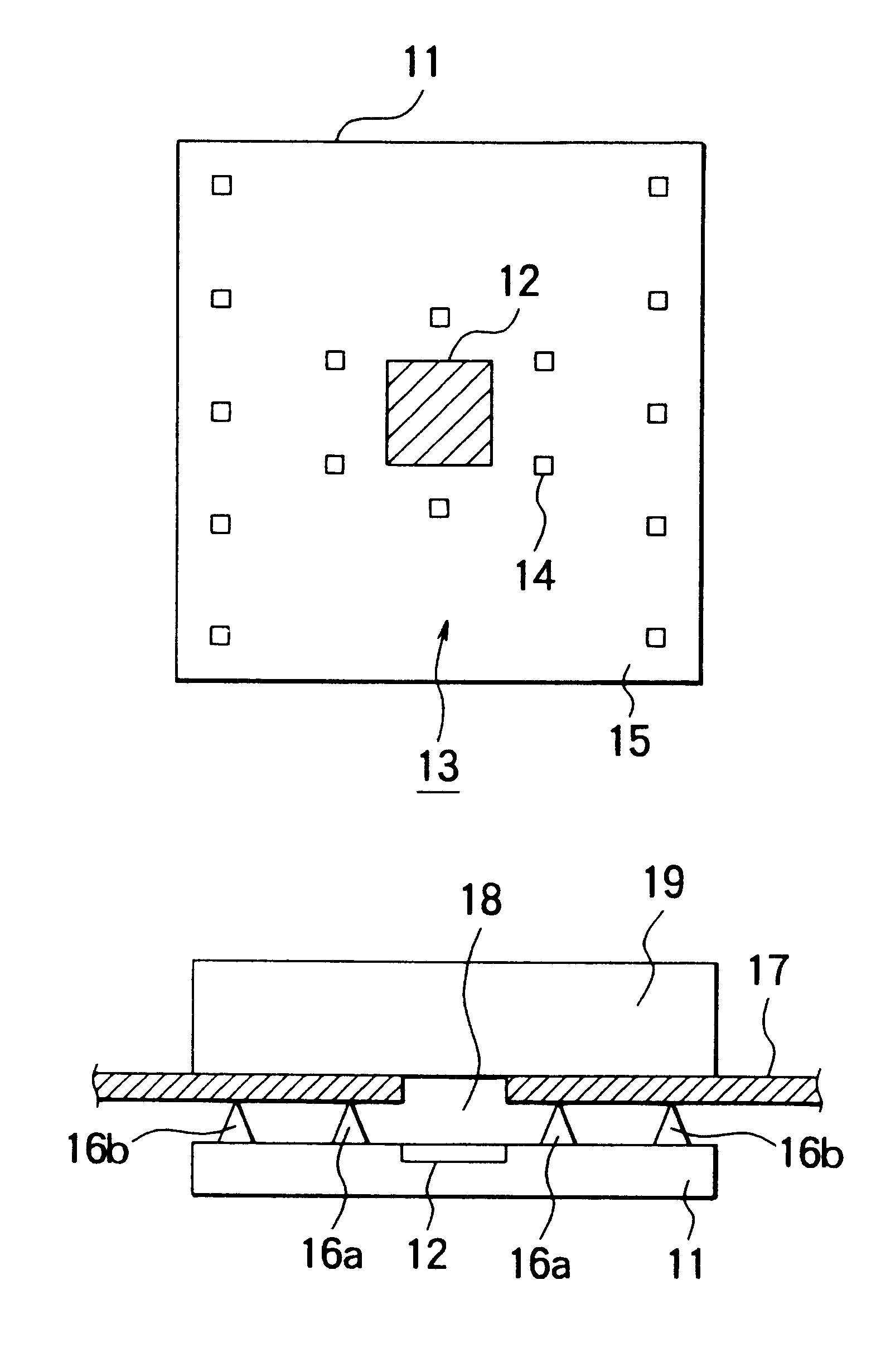
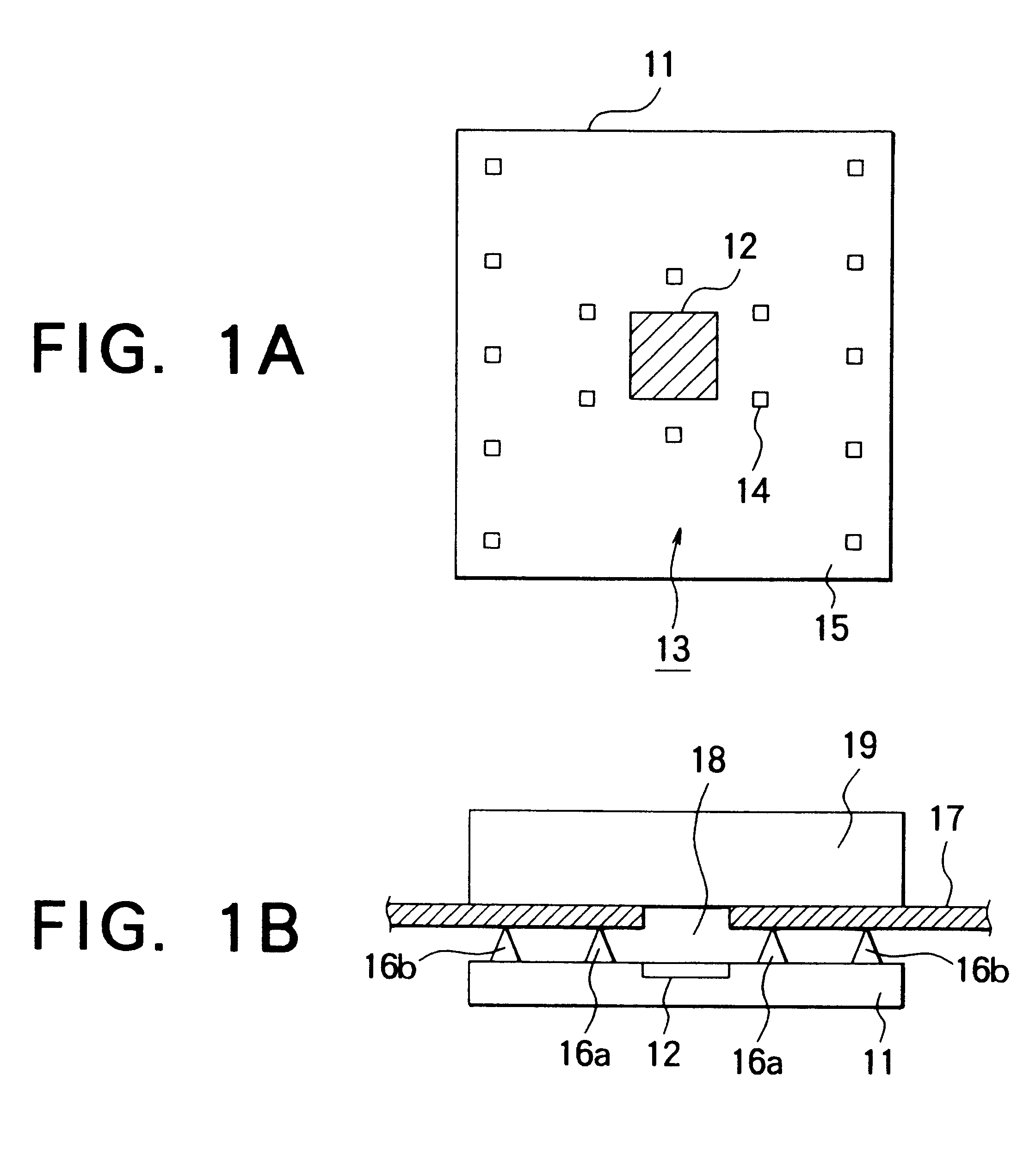
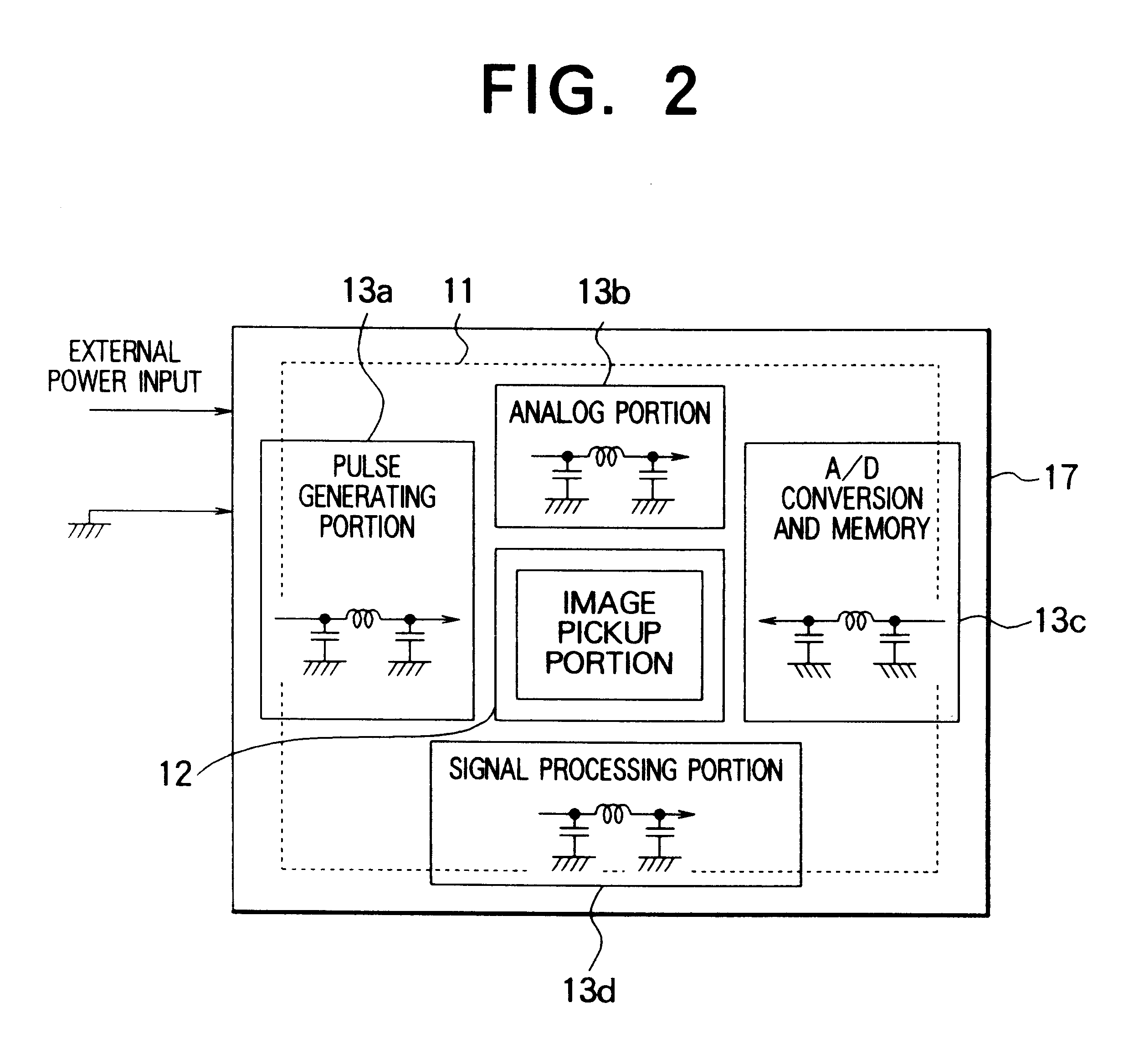
Next, with reference to the accompanying drawings, embodiments of the present invention will be described. FIGS. 1A, 1B, and 2 are schematic diagrams for explaining a first embodiment of the present invention. In FIG. 1A, reference numeral 11 represents an IC apparatus according to the first embodiment of the present invention. The IC apparatus 11 is a one-chip IC of which an image pickup portion 12 and a peripheral circuit portion 13 thereof are structured with one chip. The peripheral circuit portion 13 comprises a pulse generating portion 13a, an analog portion 13b, an A / D conversion and memory portion 13c, and a signal processing portion 13d. Thus, the image pickup portion 12 and the peripheral circuit portion 13 are composed of the transistors that can be structured as one chip, for example MOS type transistors. Electrode pads 14 are disposed on the front surface and on the periphery of the image pickup portion 12 so that the electrode pads 14 are electrically connected to the ...


PUM


Abstract

Power supplies, a ground, and so forth of an analog portion including an image pickup portion 12 are connected to electrode pads 14. Power supplies, a ground, and so forth of a digital portion are connected to electrode pads 15. Thus, various problems such as an increase of impedance of power supplies and a ground, signal crosstalk between each circuit, and noise due to internal line connections between the image pickup portion 12 and a peripheral portion 13 can be prevented.

Description

1. Field of the InventionThe present invention relates to an optical integrated circuit that integrates an image pickup device (for use with a video camera or an electronic camera) and a peripheral circuit.2. Description of the Related ArtFIGS. 7A and 7B show an IC chip for a conventional charge coupled device (CCD) as an image pickup device. The CCD comprises photo diodes 71, a horizontal CCD transferring portion 72, a vertical CCD transferring portion 73, and a signal outputting portion 74. As shown in FIG. 8, the CCD is housed in a ceramics package 81. Electrode pads of the CCD are connected with wire bonds 82. The resultant structure is packaged with a cover glass 83. As shown in FIG. 9, a CCD camera comprises a light receiving portion 91, a CCD 92, a signal processing IC 93, a CCD driving IC 94, and a noise processing IC 95.An MOS type sensor that had been used for an image pickup device as with a conventional CCD has been attractive because of improvements in sensitivity, S / N ...

Claims


Application Information

Patent Timeline
Patent Type & Authority Patents(United States)
IPC IPC(8): H01L27/00H01L27/14
CPCH01L27/14618H01L27/14623H04N5/2253H04N5/2257H01L2924/0002H04N23/57H04N23/54H01L2924/00H01L27/14
Inventor KIMURA, MASANOBU
Owner KK TOSHIBA
Why Eureka
Try Eureka