Semiconductor package having implantable conductive lands and method for manufacturing the same

a technology of semiconductor and conductive lands, which is applied in the direction of semiconductor/solid-state device details, semiconductor devices, electrical apparatus, etc., can solve the problems of reducing the electrical conductivity of the semiconductor package, and deteriorating the reliability of the semiconductor packag

Inactive Publication Date: 2002-08-06
KOSTAT SEMICON
View PDF6 Cites 202 Cited by
  • Summary
  • Abstract
  • Description
  • Claims
  • Application Information

AI Technical Summary

Problems solved by technology

Since many intermediate connecting terminals are formed within a semiconductor package in such arrangement, the length of interconnection between a bond pad in a semiconductor chip and an external connecting terminal is long, thereby deteriorating the electrical conductivity of the semiconductor package.
Moreover, the front and rear solder masks 1 and 11, which are used for insulation and protection of the conductive lands on the front and rear surfaces of the rigid substrate 10, are delaminated after a semiconductor package is completely assembled, thereby decreasing the reliability of the semiconductor package.
Defects caused by differences between thermal expansive coefficients of many parts deteriorate the reliability of the semiconductor package.
Also, various defects are caused by differences between thermal expansive coefficients of the tape film 23 and other parts packaged within the semiconductor package, thereby deteriorating the reliability of the semiconductor package.
However, for a conventional QFN package, the lead frame 49 should be formed of copper or an alloy of copper, and this lead frame 49 remains as the part of the semiconductor package after completion of assembly of the semiconductor package, thereby hindering in decreasing the thickness of the semiconductor package.
Moreover, during a singulation process for taking off individual semiconductor packages from a strip of semiconductor packages, it is very difficult to take off a semiconductor package including the lead frame 49, thereby causing many defects.

Method used


Image

  • Semiconductor package having implantable conductive lands and method for manufacturing the same
  • Semiconductor package having implantable conductive lands and method for manufacturing the same
  • Semiconductor package having implantable conductive lands and method for manufacturing the same

Examples


first embodiment

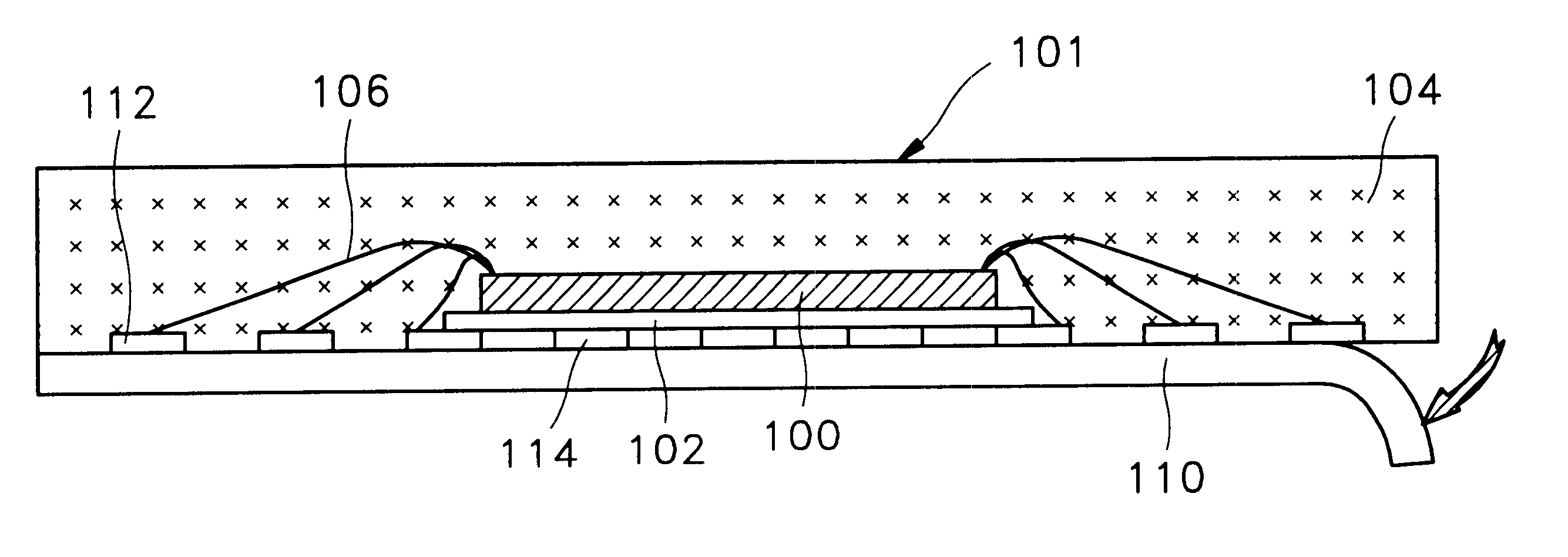
FIGS. 16 through 22 are views illustrating the structure of a semiconductor package according to a first embodiment of the present invention, and a method for manufacturing the same. Referring to FIG. 16, the semiconductor package according to the first embodiment of the present invention includes a semiconductor chip 100, a semiconductor package body 101 including a heat conductive or electrically conductive die-bonding epoxy 102, for bonding the bottom of the semiconductor chip 100, gold wires 106 and a sealing resin 104 of an epoxy mold compound, and implantable conductive lands 112 including heat sink implantable conductive lands 114.

The gold wires 106 connect the implantable conductive lands 112 to the respective bond pads of the semiconductor chip 100. The heat conductive or electrically conductive die-bonding epoxy 102 directly bonds the semiconductor chip 100 to the heat sink implantable conductive lands 114.

The structure of a semiconductor package illustrated in FIG. 17 is ...

second embodiment

FIGS. 23 through 28 are views illustrating the structure of a semiconductor package according to a second embodiment of the present invention and a method for manufacturing the same.

Referring to FIGS. 23 through 25, since the present invention uses a tape film including implantable conductive lands instead of a conventional lead frame, the structure of a QFN type semiconductor package is almost the same as that of the first embodiment, and thus a description thereof will be omitted. For clear understanding, last digits of the reference numerals are set to correspond to those used in the first embodiment.

FIG. 26 is a flowchart illustrating a method of manufacturing a semiconductor package including implantable conductive lands according to the second embodiment of the present invention. Referring to FIG. 26, a die bonding process and a wire bonding process are performed in the same manner as in the first embodiment. Next, a die-bonding epoxy is hardened while a volatile material cont...

third embodiment

e

FIGS. 29 through 34 are views illustrating the structure of a semiconductor package according to a third embodiment of the present invention and a method for manufacturing the same.

FIG. 29 is a sectional view illustrating the structure of a semiconductor package including implantable conductive lands according to the third embodiment of the present invention. A semiconductor package according to the third embodiment of the present invention is composed of a semiconductor package body 301 and implantable conductive lands 312, like the first and second embodiments. However, the internal shape of the semiconductor package body 301 is different from those of the first and second embodiments. In other words, the semiconductor package of the third embodiment does not include gold wires and die-bonding epoxy. A solder bump 308 protruding from each bond pad of a semiconductor chip 300 is provided to be directly connected to an implantable conductive land 312.

Referring to FIGS. 30 and 31, a...


PUM


Abstract

A semiconductor package having implantable conductive lands for simplifying the manufacture of the semiconductor package, reducing the manufacturing cost by reducing the price of raw materials and improving the electrical, thermal and mechanical performance of the semiconductor package, and a method for manufacturing the same are provided. The semiconductor package includes a semiconductor package body and implantable conductive lands fixed in the semiconductor package body and taken off a tape film serving as a substrate of the semiconductor package until a molding process is completed. The tape film that has served as the substrate is taken off and removed from the semiconductor package body after the molding process so that the semiconductor package body does not include a substrate therewithin.

Description

1. Field of the InventionThe present invention relates to a semiconductor package and a method for manufacturing the same, and more particularly, to a chip scale package (CSP) which does not include a lead or uses a solder ball instead of a lead.2. Description of the Related ArtRecently, electronic products such as personal computers, cellular phones and camcorders have became smaller in size and larger in processing capacity. Accordingly, a semiconductor package which is small in size, large in capacity and compliant with a fast processing speed is required. Therefore, semiconductor packages have been transformed from an insertional mounting type including a dual in-line package (DIP) into a surface mounting type including a thin small out-line package (TSOP), a thin quad flat package (TQFP) and a ball grid array (BGA).The BGA, among the surface mounting types, has attracted considerable attention since allows the size and the weight of a semiconductor package to be greatly reduced...

Claims


Application Information

Patent Timeline
Patent Type & Authority Patents(United States)
IPC IPC(8): H01L21/02H01L21/68H01L23/31H01L23/28H01L21/56H01L21/67H01L23/12H01L23/48
CPCH01L21/566H01L21/568H01L23/3107H01L2224/16245H01L2224/32225H01L2224/32245H01L2224/48091H01L2224/48227H01L2224/48237H01L2224/48247H01L2224/49171H01L2224/73265H01L2924/01046H01L2924/01078H01L2924/01079H01L2924/15311H01L2924/00014H01L24/48H01L24/49H01L2224/48233H01L2224/48253H01L2924/00H01L2224/45144H01L2924/00012H01L2924/12042H01L24/73H01L2924/181H01L2224/05554H01L2224/48257H01L24/45H01L2924/10162H01L2224/49433H01L2224/45015H01L2924/207H01L23/48
Inventor GANG, HEUNG-SU
Owner KOSTAT SEMICON
Why Eureka
Try Eureka