Semiconductor package and method for fabricating the same

a technology of semiconductor and semiconductor products, applied in the direction of semiconductor/solid-state device details, semiconductor devices, electrical apparatus, etc., can solve the problems of increasing fabrication time and cost, unable to meet the demands of lighter, thinner, shorter and smaller semiconductor products, and the height of the semiconductor package cannot be further reduced, so as to achieve efficient mounting, avoid conventional delamination, and small size

Inactive Publication Date: 2009-04-23
SILICONWARE PRECISION IND CO LTD
View PDF1 Cites 112 Cited by
  • Summary
  • Abstract
  • Description
  • Claims
  • Application Information

AI Technical Summary

Benefits of technology

[0019]Furthermore, the conductive metal layer can be made of a same material as the metal carrier, such that when the metal carrier is removed, part of the conductive metal layer can be removed at the same time, and by controlling the etch quantity of the conductive metal layer, surface of the conductive metal layer can be lower than that of the dielectric layer, thereby allowing the conductive elements to be efficiently mounted to the conductive metal layer.
[0020]Therefore, the present invention mainly comprises forming a first resist layer on a metal carrier and forming a plurality of openings in the first resist layer to expose the metal carrier such that a conductive metal layer can be formed in the openings; removing the first resist layer, forming a dielectric layer to cover one side of the metal carrier having the conductive metal layer, and forming a plurality of blind vias in the dielectric layer to expose part of the conductive metal layer; forming conductive circuit on the dielectric layer and forming conductive posts in the blind vias, wherein the conductive circuit is electrically connected with the conductive metal layer through the conductive posts; electrically connecting at least one chip to the conductive circuit; forming an encapsulant encapsulating the chip and the conductive circuit and removing the metal carrier so as to expose the dielectric layer and the conductive metal layer functioning as electrical connection terminals. Thus, a semiconductor package without chip carrier is obtained. Since the conductive circuit and the conductive metal layer functioning as electrical connection terminals are efficiently embedded in the dielectric layer through the conductive posts, the conventional delamination problem is avoided. Further, the blind vias formed in the dielectric layer have small size, thereby facilitating the fabrication process and saving the fabrication cost compared with the large-sized openings in the prior art.

Problems solved by technology

However, limited by thickness of the conventional lead frames, height of the semiconductor packages cannot be further reduced, which accordingly cannot meet demands for lighter, thinner, shorter and smaller semiconductor products.
As a result, both the fabrication time and cost are increased.
Further, as the conductive circuits only have a thickness of 5-10 μm and have a poor bonding with the encapsulant, delimination can easily occur between the terminals of the conductive circuits and the encapsulant.

Method used


Image

  • Semiconductor package and method for fabricating the same
  • Semiconductor package and method for fabricating the same
  • Semiconductor package and method for fabricating the same

Examples


first embodiment

[0027]FIGS. 2A to 2H are sectional diagrams showing a semiconductor package and a method for fabricating the same according to a first embodiment of the present invention.

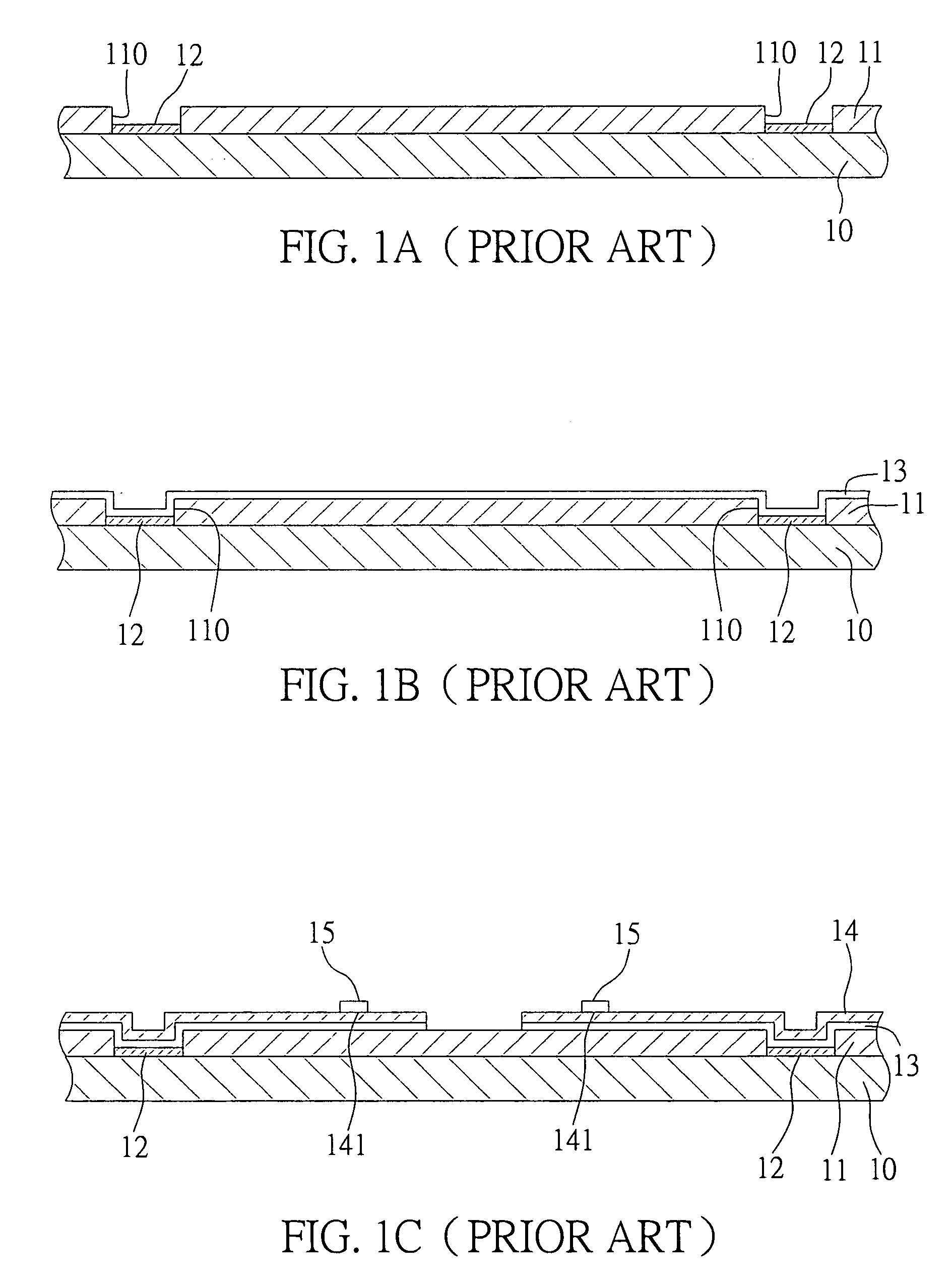
[0028]As shown in FIG. 2A, a metal carrier 20 such as a copper plate is prepared, a first resist layer 21 such as photo-resist is formed on one surface of the metal carrier 20, and a plurality of openings 210 penetrating the first resist layer 21 is formed by exposure and development so as to expose part of the metal carrier 20.

[0029]Subsequently, a conductive metal layer 22 is formed in the openings 210 of the first resist layer 21, wherein the conductive metal layer 22 comprises a die pad 221 corresponding to a chip position and electrical connection terminals 222 for electrically connecting the chip with an external device. The conductive metal layer 22 can be made of such as Au / Ni / Cu, Ni / Cu, Au / Ni / Au, Au / Ni / Pd / Au, Au / Pd / Ni / Pd and so on.

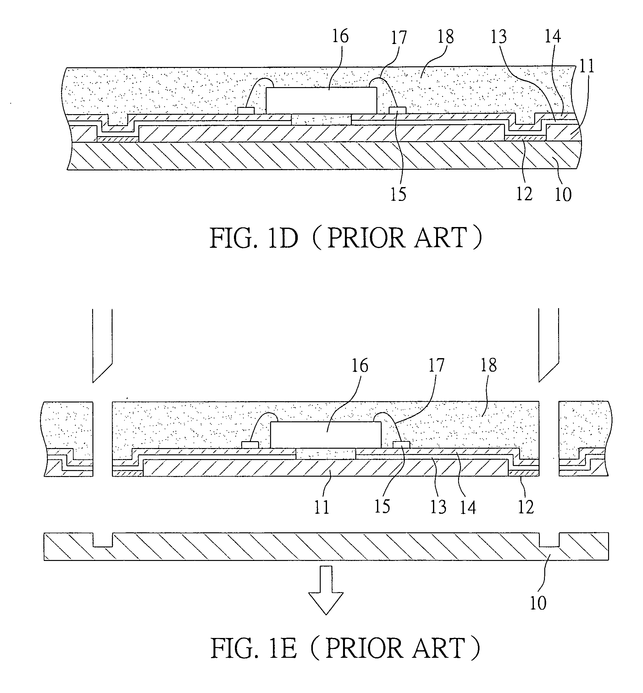
[0030]As shown in FIGS. 2B and 2C, the first resist layer 21 is removed, a d...

second embodiment

[0041]FIGS. 3A to 3C are sectional diagrams showing a semiconductor package and method for fabricating the same according to a second embodiment of the present invention. A main difference between the present embodiment and the first embodiment is an electroplating layer made of a same material as the metal carrier is formed in the openings of the first resist layer before the conductive metal layer is formed in the openings, and when the metal carrier is removed, the electroplating layer is also removed so as to make exposed surface of the conductive metal layer be lower than surface of the dielectric layer.

[0042]As shown in FIG. 3A, a first resist layer 31 is formed on a metal carrier 30 (for example a copper plate) and a plurality of openings 310 is formed in the first resist layer 31 to expose the metal carrier 30. Subsequently, an electroplating layer 300 made of the same material (copper) as the metal carrier 30 is formed in the openings 310 by electroplating and then a conduc...

third embodiment

[0045]FIGS. 4A and 4B are sectional diagrams showing a semiconductor package and method for fabricating the same according to a third embodiment of the present invention.

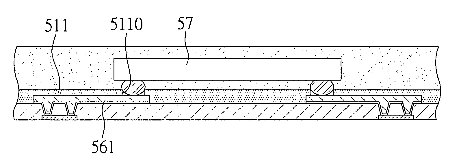
[0046]A main difference of the present embodiment from the above-described embodiments is the conductive metal layer 42 is made of a same material as the metal carrier 40 such that when the metal carrier 40 is removed by etching, part of the conductive metal layer 42 can also be removed. By controlling etch quantity of the conductive metal layer 42 (approximately 10 μm etch depth), surface of the conductive metal layer 42 can be made to be lower than that of the dielectric layer 43, thereby allowing the conductive elements 480 to be efficiently mounted to the conductive metal layer 42.


PUM

PropertyMeasurementUnit
thicknessaaaaaaaaaa
diameteraaaaaaaaaa
diameteraaaaaaaaaa

Abstract

This invention provides a semiconductor package and a method for fabricating the same. The method includes: forming a first resist layer on a metal carrier; forming a plurality of openings penetrating the first resist layer; forming a conductive metal layer in the openings; removing the first resist layer; covering the metal carrier having the conductive metal layer with a dielectric layer; forming blind vias in the dielectric layer to expose a portion of the conductive metal layer; forming conductive circuit on the dielectric layer and conductive posts in the blind vias, such that the conductive circuit is electrically connected to the conductive metal layer via the conductive posts; electrically connecting at least one chip to the conductive circuit; forming an encapsulant for encapsulating the chip and the conductive circuit; and removing the metal carrier, thereby allowing a semiconductor package to be formed without a chip carrier. Given the conductive posts, both the conductive circuit and conductive metal layer are efficiently coupled to the dielectric layer to prevent delamination. Further, downsizing the blind vias facilitates the fabrication process and cuts the fabrication cost.

Description

BACKGROUND OF THE INVENTION[0001]1. Field of the Invention[0002]The present invention relates generally to a semiconductor package and method for fabricating the same, and more particularly to a semiconductor package without chip carrier and method for fabricating the same.[0003]2. Description of Related Art[0004]In a conventional semiconductor package, a lead frame is used as a chip carrier, which comprises a die pad and a plurality of leads formed around periphery of the die pad. A semiconductor chip is adhered to the die pad and electrically connected with the leads by bonding wires, and further, the chip, the die pad, the bonding wires and inner side of the leads are encapsulated by a package resin so as to form a semiconductor package with lead frame.[0005]There are various kinds of semiconductor packages with lead frame. For example, a QFP (Quad Flat Package) semiconductor package uses outer leads for electrical connection with an external device while a QFN (Quad Flat Non-lea...

Claims


Application Information

Patent Timeline
Patent Type & Authority Applications(United States)
IPC IPC(8): H01L23/48H01L21/00
CPCH01L21/486H01L2924/01033H01L23/3128H01L23/49827H01L24/16H01L24/48H01L24/97H01L2221/68345H01L2224/16237H01L2224/48091H01L2224/48227H01L2224/97H01L2924/01029H01L2924/01046H01L2924/01078H01L2924/01079H01L2924/01082H01L2924/15311H01L21/6835H01L2924/00014H01L2224/85H01L2924/181H01L2924/00012H01L2224/45099H01L2224/45015H01L2924/207
Inventor LEE, CHUN-YUANHUANG, CHIEN PINGLAI, YU-TINGHSIAO, CHENG-HSUKE, CHUN-CHI
Owner SILICONWARE PRECISION IND CO LTD
Why Eureka
Try Eureka