Circuit board having deposit holes

Inactive Publication Date: 2005-06-09
OPTIMUM CARE INT TECH
View PDF9 Cites 44 Cited by
  • Summary
  • Abstract
  • Description
  • Claims
  • Application Information

AI Technical Summary

Benefits of technology

[0006] further reducing the board's

Problems solved by technology

However, the abovementioned construction scheme for an electronic board only arranged electronic components on the selected surface of the circuit board, and conventional electronic componen

Method used


Image

  • Circuit board having deposit holes
  • Circuit board having deposit holes
  • Circuit board having deposit holes

Examples


Example

[0016] Hereinbelow, the structural features, embodiments, and objectives of the present invention are described in details with reference to the attached drawings:

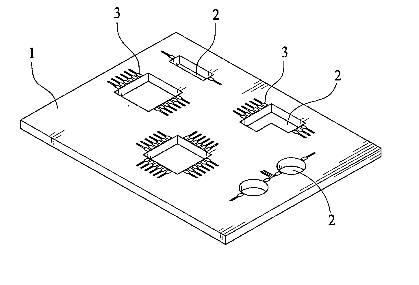
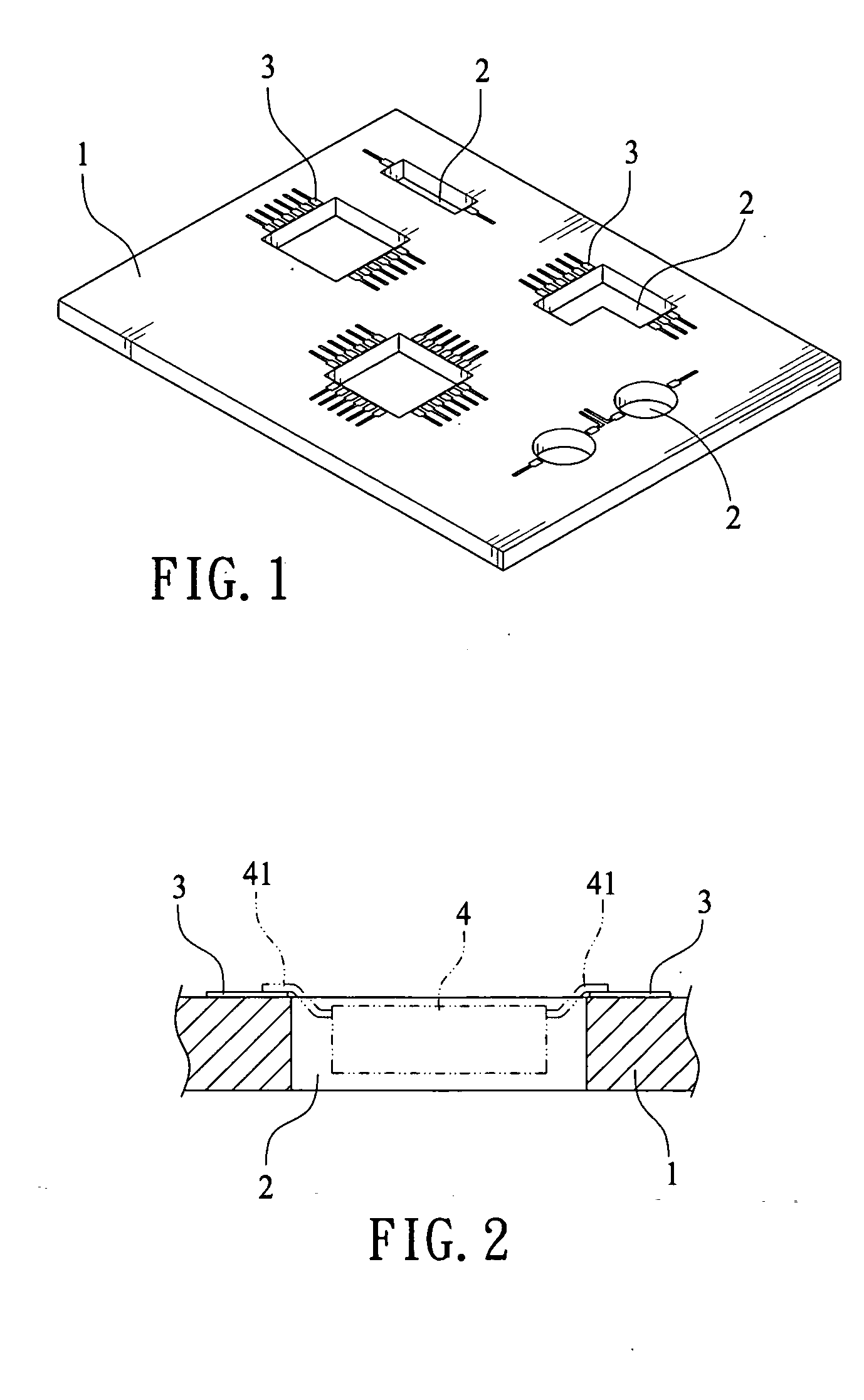
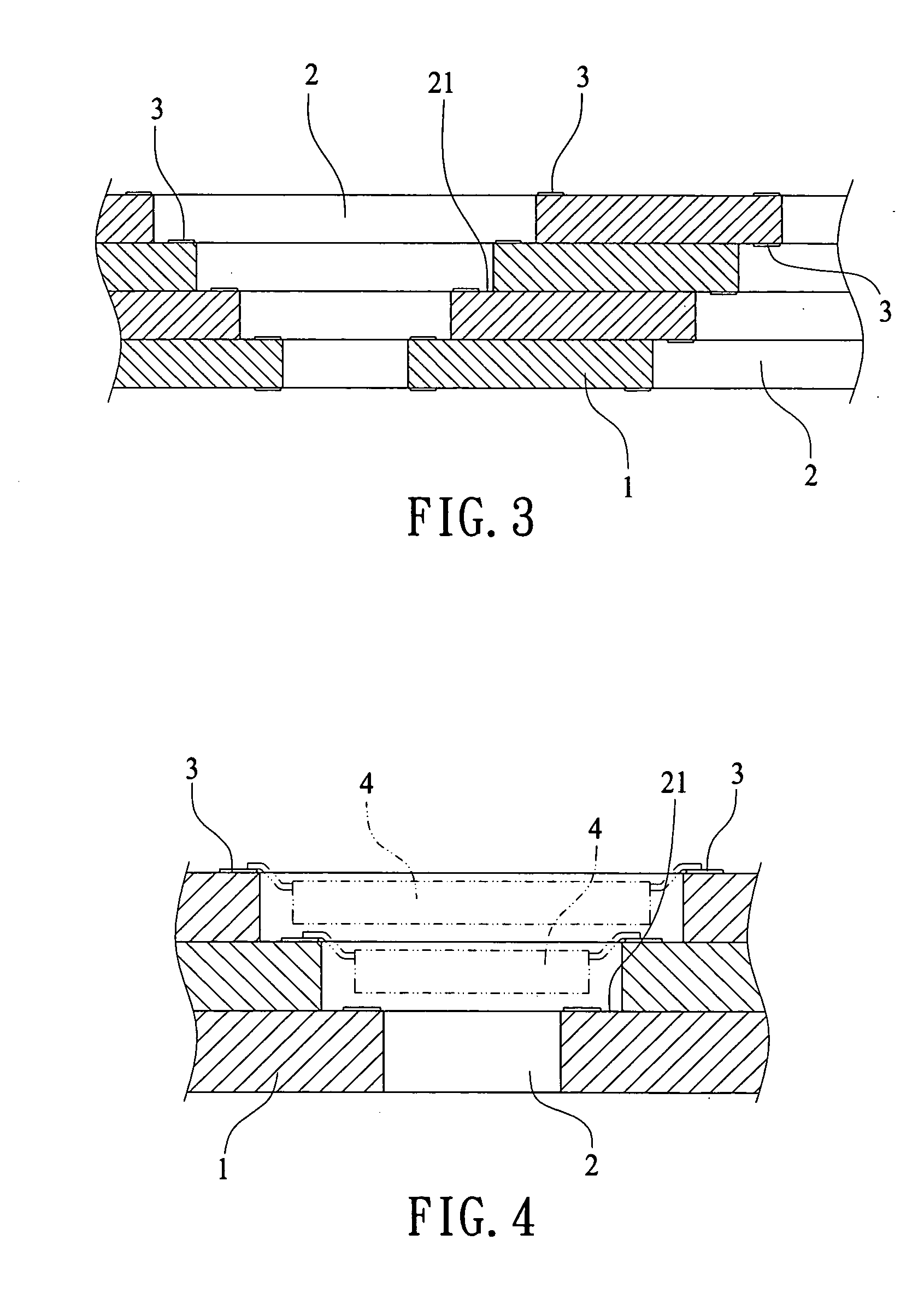
[0017] As illustrated by the attached drawings, the present invention relates to the structural design of “circuit boards having deposit holes”, wherein said circuit boards cover motherboards, display cards, memory cards, network cards, along with the circuit boards (cards) for mobile phones, translators, or other special purposes. The embodiments of the present invention include:

[0018] As shown in FIGS. 1 and 2, one or more deposit holes 2 penetrate the circuit board 1 at locations specified by the layout of the final electronic device or circuit. Furthermore, the deposit holes 2 can either be designed with regular shapes, such as a rectangle or a circle, or shaped randomly. In addition, in accordance with the electronic components to be placed in the deposit holes 2, multiple circuit contacts 3 are fixed on one or both...


PUM


Abstract

The present invention relates to the structural design of a circuit board having deposit holes. The design is to allocate one or more deposit holes that are either caved in or penetrate through the board at locations specified by the spatial layout, as well as to set step-like holes on a multilayer circuit board. On the panel surrounding the edge of the deposit holes, circuit contacts are provided for connecting electronic components (for example IC transistors, connectors, resistors, capacitors, or other circuit boards), such that when placed in deposit holes, they can be welded or fixed via the circuit contacts.

Description

FIELD OF THE INVENTION [0001] The present invention is related to the design of a circuit board having deposit holes, specifically, to an improved design for a circuit board (card) structure that can be widely applied in various circuit boards (cards), such that electronic components can make the most effective use of the space. DESCRIPTION OF PRIOR ART [0002] Current electronic related products have a design trend towards having features of light weight compactness and sophistication, for example, Personal Digital Assistant (PDA), mobile phone, notebook, language translator, handy drive, and MP3 player etc. The conventional way to construct the main portion of these above-mentioned electronic products, i.e. the circuit board, is to design electronic circuits (printed circuits) on the circuit board surface, then arrange many electronic components (such as IC transistor, electric connector, resistor, capacitor, or light emitting diode) with specific function to be welded on the circu...

Claims


Application Information

Patent Timeline
IPC IPC(8): H05K1/18
CPCH05K1/182H05K1/183H05K2201/09036H05K2201/10689H05K2201/10515H05K2201/10651H05K2201/09845
Inventor LIEN, JEFFREY
Owner OPTIMUM CARE INT TECH
Why Eureka
Try Eureka