Method for manufacturing lens for led package

Inactive Publication Date: 2008-10-16
ALTI ELECTRONICS
View PDF8 Cites 29 Cited by
  • Summary
  • Abstract
  • Description
  • Claims
  • Application Information

AI Technical Summary

Benefits of technology

[0014]It is an object of the present invention to provide a method for manufacturing a lens for an LED package in which a manufacturing process is simple. It is another object of the present invention to provide a method for manufacturing a lens for an LED package in which the thickness and volume of a backlight unit employing the LED package are reduced and the brightness is increased.
[0024]The upper plate jig moves down to the lower plate jig to press the dome lens, the concave groove is formed corresponding to the height of a press arm of the upper plate jig for restricting the pressing range.

Problems solved by technology

The LED package has low light efficiency because a total reflection of light occurs in an interface between a molded upper surface and an air and so lots of light go back to an inside of the LED package.
However, in such a conventional LED package having the dome lens, a process for manufacturing the dome lens and a process for attaching the dome lens to the LED package are very complicated.
In addition, since an interface and a fine gape are formed between the dome lens and the LED package, light efficiency is low due to a refraction index difference.

Method used


Image

  • Method for manufacturing lens for led package
  • Method for manufacturing lens for led package
  • Method for manufacturing lens for led package

Examples


Embodiment Construction

[0038]Reference will now be made in detail to the embodiments of the present invention, examples of which are illustrated in the accompanying drawings, wherein like reference numerals refer to the like elements throughout. The embodiments are described below in order to explain the present invention by referring to the figures.

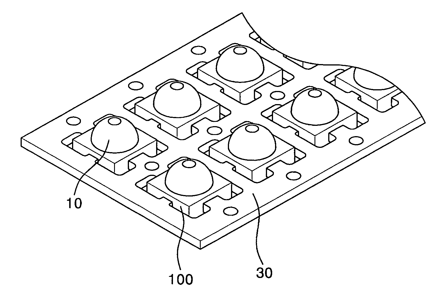
[0039]According to the present invention, an LED chip is mounted to a lead frame through a die bonding (D / B) and wire boding (W / B), and the LED chip is molded by silicon. A dome lens of a dome shape is manufactured on the LED package by silicon. The dome lens is manufactured by a dispensing technique or a printing technique. The LED package having the dome lens is located between upper and lower plate jigs, and the upper plate jig moves down toward the lower plate jig to thereby forming a concave groove in the dome lens. In this pressed state, the concave grove is cured.

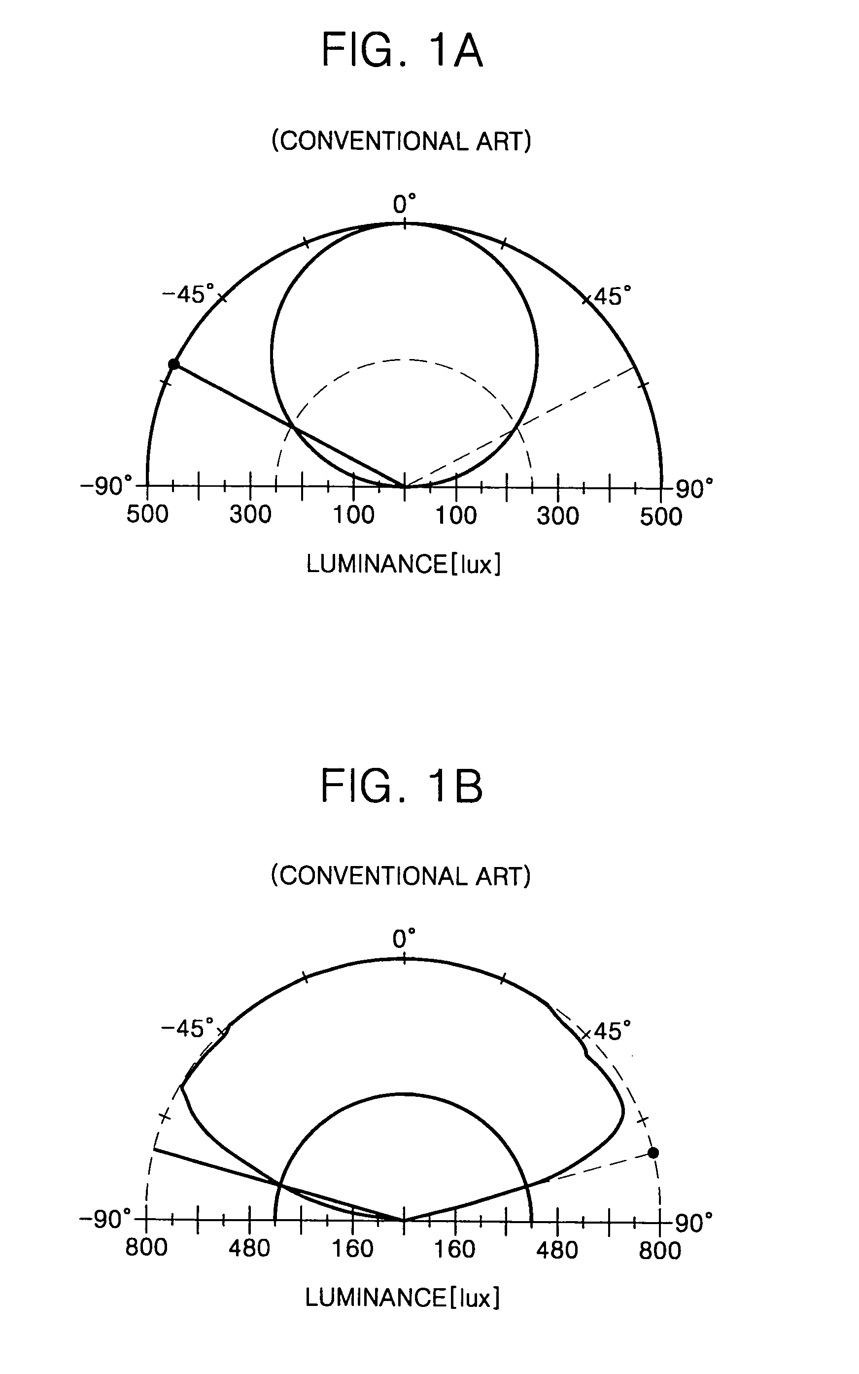
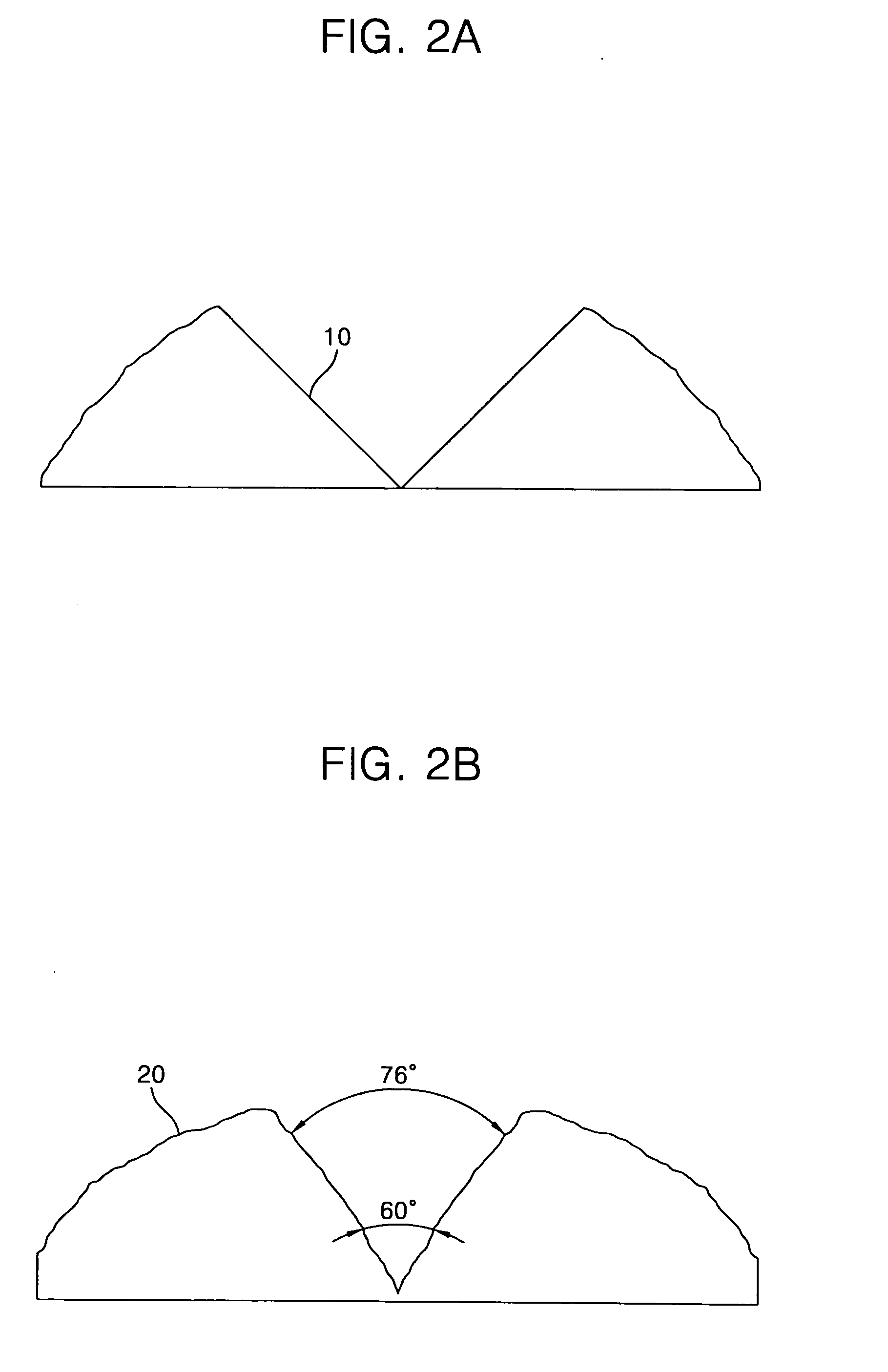
[0040]FIG. 2A is a side view illustrating a dome lens according to an exemplary embodiment ...


PUM


Abstract

A method for manufacturing a lens for a light emitting diode (LED) package is disclosed. The method for manufacturing a lens for an LED package includes: forming a dome lens on each of a plurality of LED packages placed on a fixing plate, the dome lens made of silicon; forming a concave groove in the dome lens by using a jig for pressing the dome lens; curing the dome lens; and removing the LED packages from the fixing plate.

Description

CROSS-REFERENCE TO RELATED APPLICATION[0001]This application claims priority to and the benefit of Korean Patent Application No. 2007-35417, filed on Apr. 11, 2007, the disclosure of which is incorporated herein by reference in its entirety.BACKGROUND OF THE INVENTION[0002]1. Field of the Invention[0003]The present invention relates to a light emitting diode (LED) package, and more particularly, to a method for manufacturing a lens for an LED package in which a manufacturing process is simplified.[0004]2. Description of the Related Art[0005]A liquid crystal display (LCD) device displays an image such that an electric power is applied to each pixel to change an alignment of liquid crystal molecules. An LCD device is a non-emissive display device and so needs a backlight unit which uniformly irradiates light to a display panel so that it can be used even in a dark place.[0006]The backlight unit comprises a light source like a fluorescent lamp or a light emitting diode (LED), a light g...

Claims


Application Information

Patent Timeline
IPC IPC(8): H01L33/00H01L33/50H01L33/56H01L33/58H01L33/62
CPCG02B27/0955H01L33/58G02B19/0014G02B19/0061B29D11/00
Inventor KIM, DONG-SOOCHOI, HWA-KYUNGYOON, YOUNG-SEOK
Owner ALTI ELECTRONICS
Why Eureka
Try Eureka