Image display device

a display device and image technology, applied in the direction of static indicating devices, instruments, transportation and packaging, etc., can solve the problems of increasing manufacturing costs and conventional problems, and achieve the effect of increasing manufacturing costs and increasing manufacturing costs

Inactive Publication Date: 2005-01-13
HITACHI DISPLAYS
View PDF9 Cites 111 Cited by
  • Summary
  • Abstract
  • Description
  • Claims
  • Application Information

AI Technical Summary

Benefits of technology

[0007] Generally, the OLED driving TFT 102 is a polycrystalline silicon TFT, which is varied more significantly in characteristics than the single crystalline silicon transistor. Particularly, the polycrystalline silicon TFT has a large variation of the threshold voltage Vth. The above conventional technique proposes a solution for the conventional problem that such a variation often occurs in display images.
[0008] However, the conventional technique must use four transistors and two capacitors per pixel to cancel the variation of the threshold voltage Vth as described above. The four transistors are used for a driving TFT 102, a reset switch 106, an OLED switch 107, and a write switch 103, and the two capacitors are used for a write capacitor 104 and a memory capacitor 105. Because such many elements are needed for each pixel in the conventional technique, yields of the electro-luminescent display devices come to fall, thereby the manufacturing cost increases. This has been a conventional problem. And, this problem has been caused by current leaks from transistor gate insulator films and each insulator film between capacitors that have resulted in point defects, as well as line defects in some cases to occur in electro-luminescent display devices.
[0009] The above conventional problem that yields of the electro-luminescent display elements fall due to the use of four transistors and two capacitors per pixel, thereby the manufacturing cost increases can be solved by providing the subject image display device with illuminating state controlling means for collectively controlling selection of the illuminating/not-illuminating state for each display part in which a display signal voltage is written and constant voltage supplying means for supplying a constant voltage to each pixel through a signal line. The image display device comprises a pixel having an electro-lum...

Problems solved by technology

Because such many elements are needed for each pixel in the conventional technique, yields of the electro-luminescent display devices come to fall, thereby the manufacturing cost increases.
This has been a conventional problem.
And, this p...

Method used


Image

  • Image display device
  • Image display device
  • Image display device

Examples


first embodiment

[0030] Hereunder, the first embodiment of the present invention will be described with reference to FIGS. 1 through 5.

[0031] At first, an overall configuration of this first embodiment will be described with reference to FIG. 1.

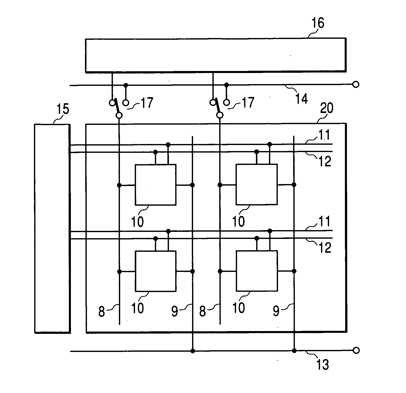
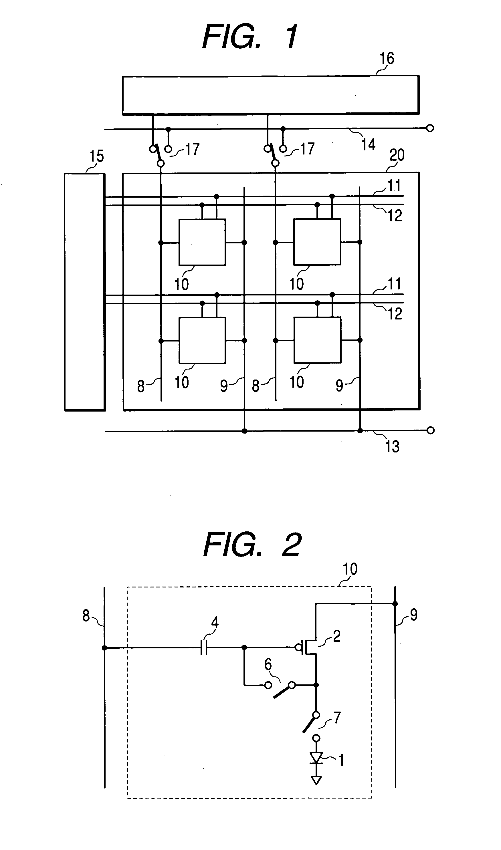
[0032]FIG. 1 shows an overall circuit diagram of an organic EL (electro-luminescent) display panel in this first embodiment. Pixels 10 are disposed like a matrix in a display area 20 and a signal line 8, a reset gate line 11, an OLED gate line 12, and a power supply line 9 are connected to each of the pixels 10. One end of the signal line 8 is connected to a signal voltage generation circuit 16 through a signal line switch 17. One end of each of the reset gate line 11 and the OLED gate line 12 is connected to a scanning circuit 15. One end of every power supply line 9 is connected to a power input line 13 and the signal line switch 17 switches the signal line 8 between the signal voltage generation circuit 16 and the constant voltage input line 14.

[0033] W...

second embodiment

[0054] Next, the second embodiment of the present invention will be described with reference to FIG. 6.

[0055] Basically, both configuration and operation of this second embodiment is the same as those of the first embodiment except for the pixel structure. In this embodiment, therefore, the pixel structure will be described while the description for the same items as those in the first embodiment is omitted.

[0056]FIG. 6 shows a circuit diagram of a pixel of an organic EL display panel in the second embodiment of the present invention.

[0057] Each pixel 30 is provided with an organic EL element 1 used as an electro-luminescent element. The cathode terminal of the organic EL element 1 is connected to a common ground. The anode terminal of the element 1 is connected to a power supply line 9 through an OLED switch 7 and a channel of a driving TFT 2. The gate of the driving TFT 2 is connected to the signal line 8 through the storage capacitor 34 and a reset switch 6 is provided between...

third embodiment

[0059] Hereunder, the third embodiment of the present invention will be described with reference to FIGS. 7 through 11.

[0060] At first, an overall configuration of an organic EL display panel in this third embodiment will be described with reference to FIG. 7. Pixels 40 are disposed like a matrix in a display area 46. And, a signal line 8, a reset gate line 11, and a power supply line 49 are connected to each of the pixels 40. One end of the signal line 8 is connected to a signal voltage generation circuit 16 through a signal switch 17 and one end of the reset gate line 11 is connected to the scanning circuit 45. The power supply lines 49 are all connected to a power input line 43 through a power supply line switch 41 respectively. Each of the power supply line switches 41 is controlled by the scanning circuit 45 while the signal line switch 17 switches the signal line 8 between the signal voltage generation circuit 16 and the constant voltage input line 14.

[0061] While many pixel...


PUM


Abstract

Disclosed herewith an image display device capable of displaying high quality images and preferred for reducing the manufacturing cost. The image display device is provided with illuminating state controlling state for controlling the illuminating state or non-illuminating state and constant voltage supply for supplying a constant voltage to each pixel through a signal line when the illuminating state is selected for the pixel.

Description

PRIORITY CLAIM [0001] This application claims priority under 35 U.S.C. §119 to Japanese patent application P-2003-13690 filed May 15, 2003 the entire disclosure of which is hereby incorporated by reference. FIELD OF THE INVENTION [0002] The present invention relates to a high quality image display device, more particularly to an image display device preferred for cost reduction. BACKGROUND OF THE INVENTION [0003] Hereunder, conventional techniques related to such image display devices will be described briefly with reference to FIGS. 18 and 19. [0004]FIG. 18 shows a circuit diagram of a pixel of an electro-luminescent display device manufactured according to a conventional technique. While pixels are disposed like a matrix in the display area of the electro-luminescent display device, only one pixel is shown in FIG. 18 to simplify the description. Each pixel 110 is provided with an organic EL (Electro-Luminescent) element 101 provided as an electro-luminescent element and the cathod...

Claims


Application Information

Patent Timeline
IPC IPC(8): G09G3/20H01L51/50G09G3/30H05B33/14
CPCG09G2300/0819G09G2300/0842G09G2300/0861G09G2300/0852H01L27/3276G09G3/3233G09G3/3291H01L27/3244G09G2310/0259H10K59/12H10K59/131A61G7/047A61G7/05A61G2203/70
Inventor AKIMOTO, HAJIMEKAGEYAMA, HIROSHISHIBA, TAKEO
Owner HITACHI DISPLAYS
Why Eureka
Try Eureka