Method and apparatus of testing memory device power and ground pins in an array assembly platform

a technology of array assembly platform and memory device, which is applied in the direction of individual semiconductor device testing, semiconductor/solid-state device testing/measurement, instruments, etc., can solve the problems of increasing the likelihood of pin/ball breakage, adding an additional risk of injecting failures into the integrated circuit device, and additional components which may be susceptible to failures

Inactive Publication Date: 2003-04-08
MICRON TECH INC
View PDF4 Cites 22 Cited by
  • Summary
  • Abstract
  • Description
  • Claims
  • Application Information

AI Technical Summary

Problems solved by technology

Each act of human intervention and each act of inserting and removing a wafer, integrated circuit die, or packaged integrated circuit from a piece of test equipment adds an additional risk for injecting failures into the integrated circuit device.
Packaged integrated circuits include an additional component which may be susceptible to failure.
However, the insertion and re-insertion of devices into various test sockets increases the likelihood of pin / ball breakage.

Method used


Image

  • Method and apparatus of testing memory device power and ground pins in an array assembly platform
  • Method and apparatus of testing memory device power and ground pins in an array assembly platform

Examples


Embodiment Construction

One or more specific embodiments of the present invention will be described below. In an effort to provide a concise description of these embodiments, not all features of an actual implementation may be described in the specification. It should be appreciated that in the development of any such actual implementation, as in any engineering or design project, numerous implementation-specific decisions are made to achieve the developers' specific goals, such as compliance with system-related and business-related constraints, which may vary from one implementation to another. Moreover, it should be appreciated that such a development effort might be complex and time consuming, but would nevertheless be a routine undertaking of design, fabrication, and manufacture for those of ordinary skill having the benefit of this disclosure.

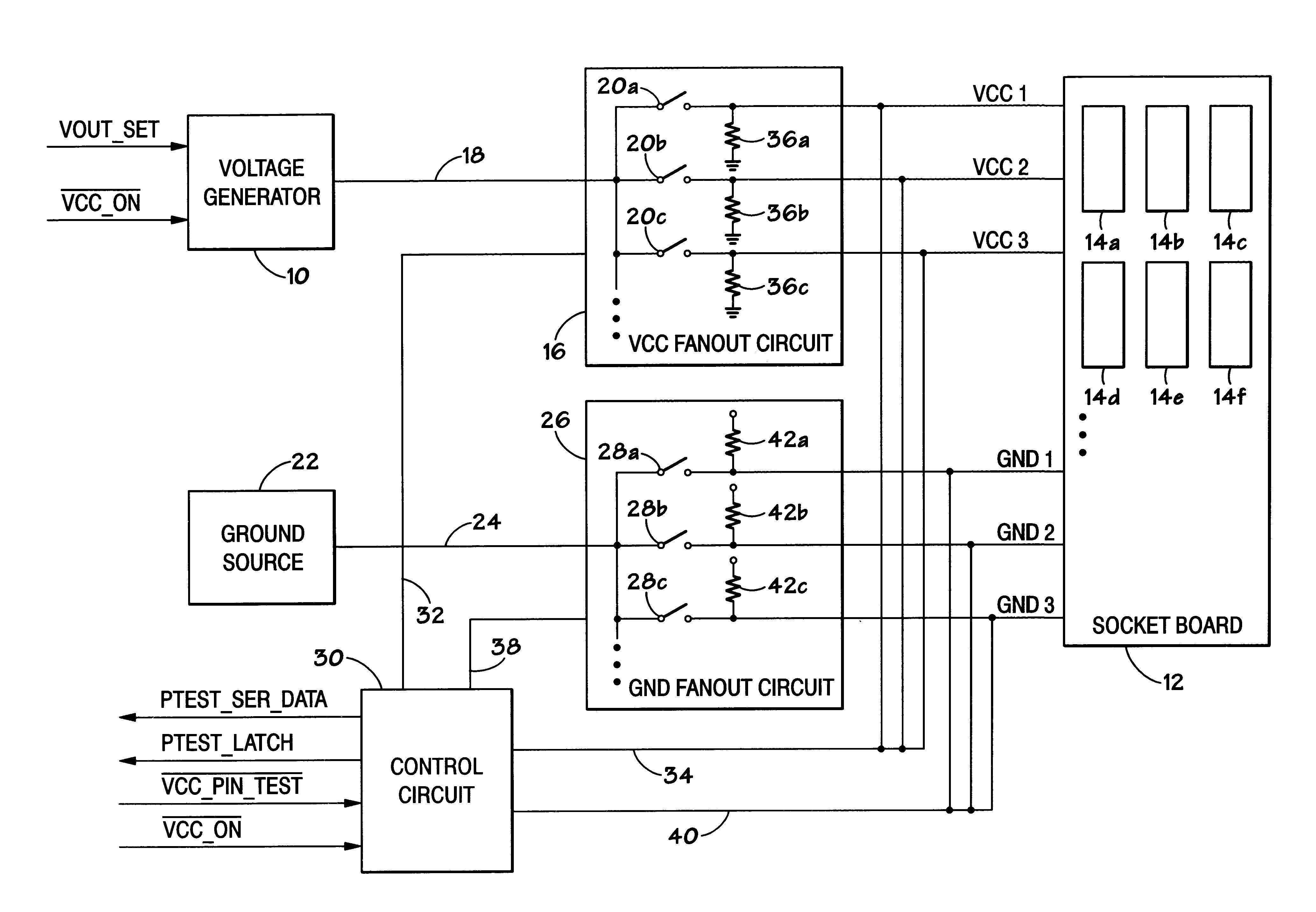
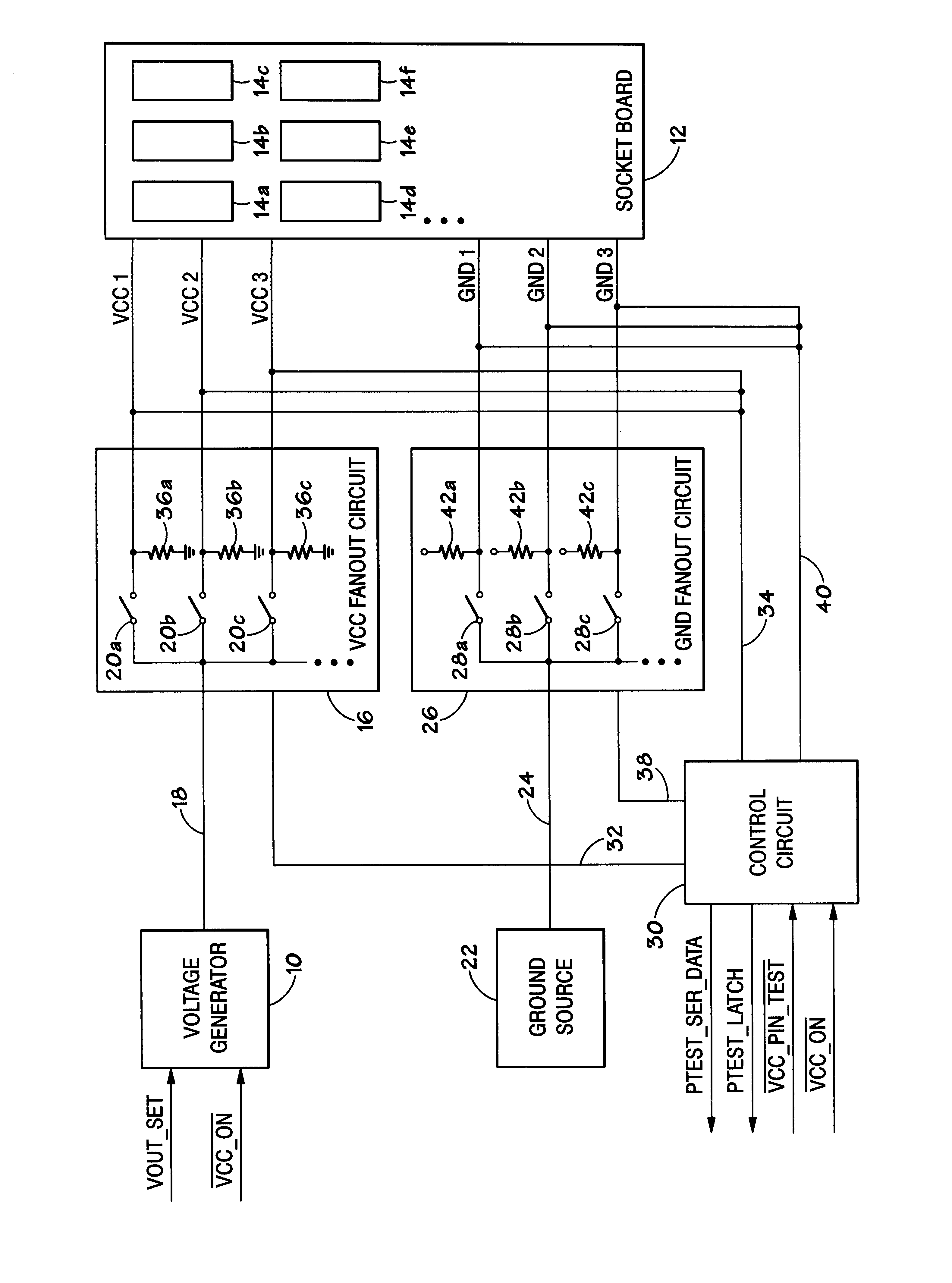
After wafer fabrication, visual inspection, and electrical tests, functional or electrically good integrated circuit devices are identified for use in a circuit ...


PUM


Abstract

An apparatus and technique for performing continuity tests of power and ground pins on a packaged integrated circuit. The technique includes using a first and second fanout circuit each including a number of signal paths. Each signal path includes a switch and corresponds to a power or ground socket on a board configured to hold a number of integrated circuit packages. The fanout circuits allow full device testing, as well as testing of individual pins. By controlling the state of the switches, power and ground may be selectively supplied to power and ground pins to check the continuity of the signals from the integrated circuit device within the package to the external pins provided to route the signal to an external device.

Description

1. Field of the InventionThe present invention relates generally to integrated circuit device assembly and, more particularly, to testing an integrated circuit device for open circuits and short circuits in the power and ground pins.2. Description of the Related ArtThis section is intended to introduce the reader to various aspects of art which may be related to various aspects of the present invention which are described and / or claimed below. This discussion is believed to be helpful in providing the reader with background information to facilitate a better understanding of the various aspects of the present invention. Accordingly, it should be understood that these statements are to be read in this light, and not as admissions of prior art.Integrated circuits are generally mass produced by fabricating thousands of identical circuit patterns on a single semiconductor wafer and subsequently dividing them into identical die or chips. To produce the integrated circuit, many commonly k...

Claims


Application Information

Patent Timeline
Patent Type & Authority Patents(United States)
IPC IPC(8): G01R1/073
CPCG01R1/07385
Inventor HEBERT, DAVEREMMERDEN, DAVEREICHLE, DAVECHADWICK, GARY
Owner MICRON TECH INC
Why Eureka
Try Eureka