

Substrate processing apparatus and method
a substrate processing and substrate technology, applied in the direction of instruments, charge manipulation, furniture, etc., can solve the problems of short transfer time for wafers, inconvenient evaluation of process recipes corresponding to inspections, and deterioration of system outpu
- Summary
- Abstract
- Description
- Claims
- Application Information
AI Technical Summary
Benefits of technology
Problems solved by technology
Method used
Image

Examples
Embodiment Construction
Next, embodiments of the present invention will be described.
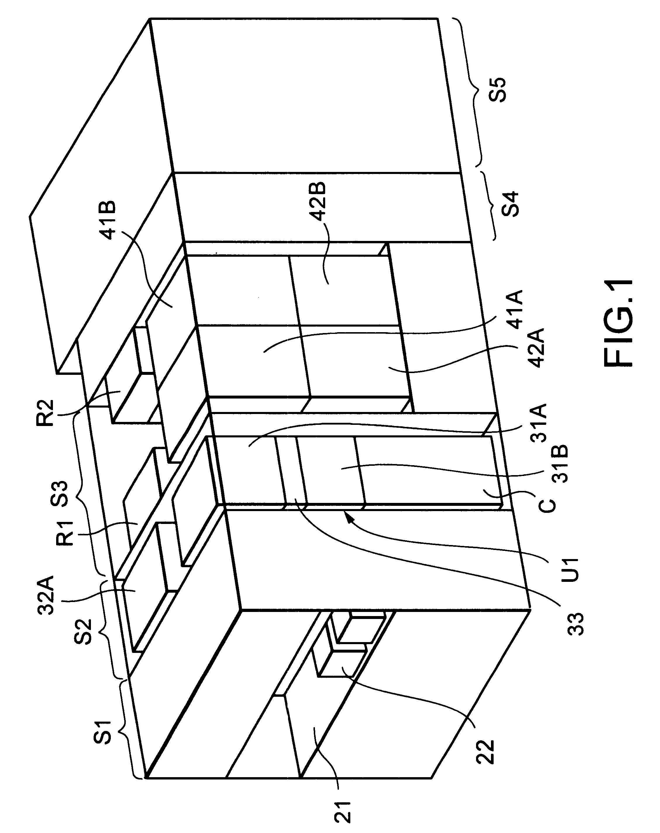
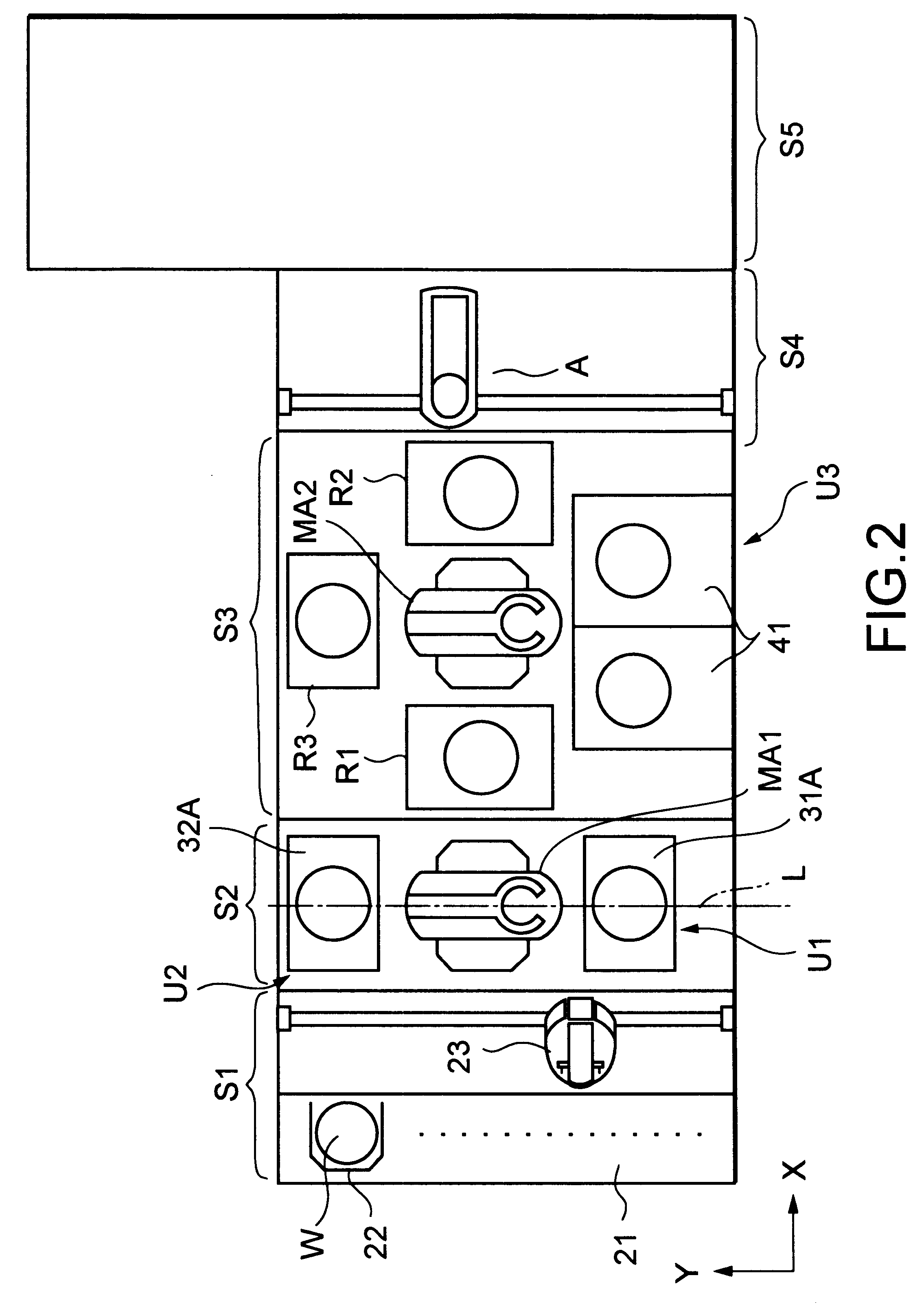
FIG. 1 is a schematic, exploded perspective view showing the interior of an embodiment of the present invention. FIG. 2 is a schematic plan view of the embodiment. In FIGS. 1 and 2, S1 represents a cassette station. S2 represents an inspecting station that performs a particular inspection for a wafer W. S3 represents a processing station that performs substrate processes such as a resist coating process, a developing process, and so forth for a wafer W. S4 represents an interface station. S5 represents an aligner.
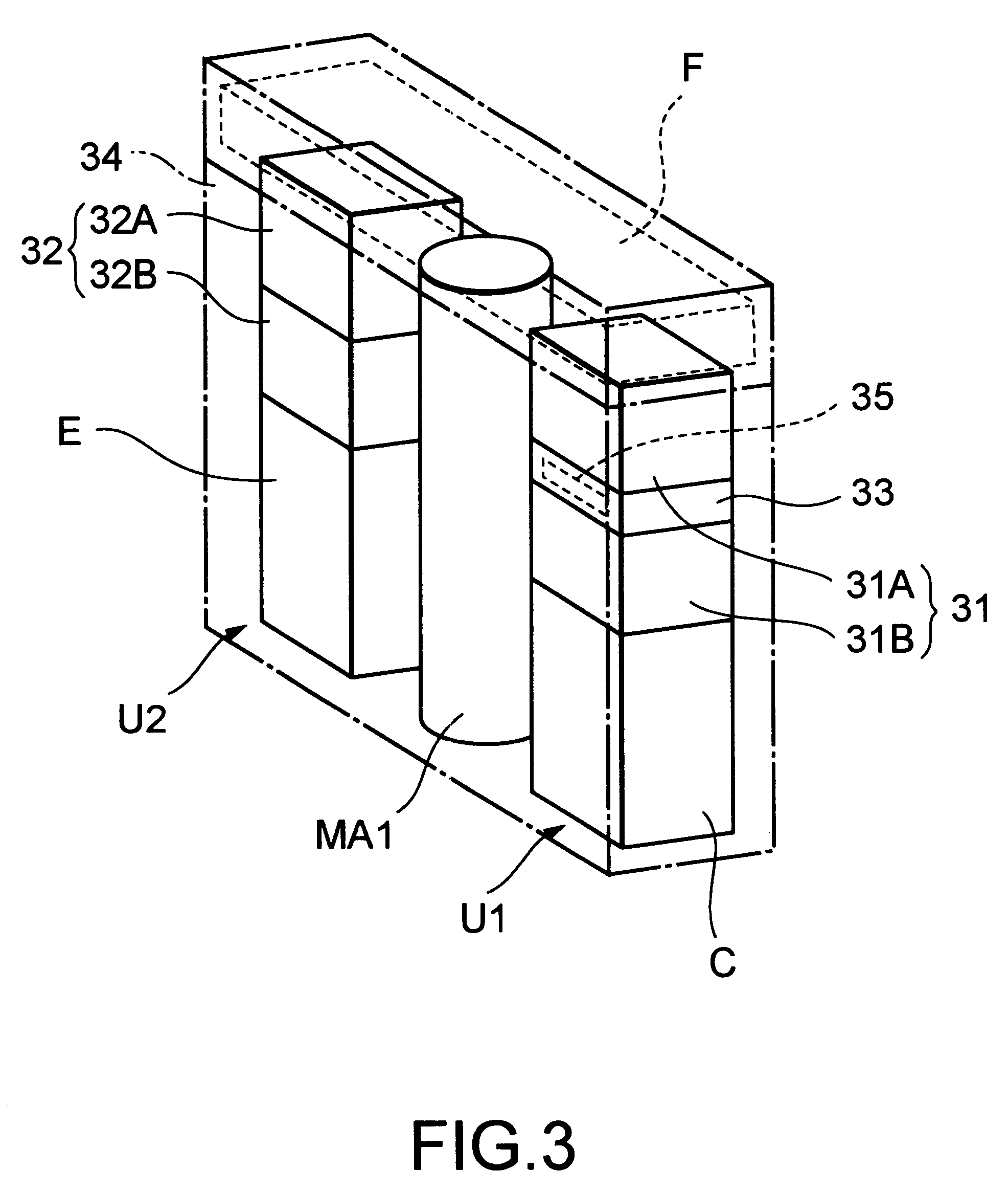
The cassette station S1 has a cassette stage 21, a cassette 22, and a transfer mechanism 23. The cassette stage 21 is a holding portion that holds wafer cassettes (hereinafter referred to as cassettes) that are for example four substrate cassettes. Each cassette contains a plurality of substrates (for example, 25 wafers). Each cassette 22 is placed on the cassette stage 21. The transfer mechanism 23 is a transferr...
PUM
| Property | Measurement | Unit |
|---|---|---|
| temperature | aaaaa | aaaaa |
| temperature | aaaaa | aaaaa |
| time | aaaaa | aaaaa |
Abstract
Description
Claims
Application Information