Methodology and apparatus using real-time optical signal for wafer-level device dielectrical reliability studies

a real-time optical signal and reliability study technology, applied in the field of system and method for testing the reliability of integrated circuit structures, can solve the problems of introducing more uncertainties and limitations for failure time detection, affecting the reliability of traditional dielectric time-to-breakdown reliability stress, and affecting the reliability of traditional dielectric time-to-breakdown stress

Inactive Publication Date: 2004-09-07
GLOBALFOUNDRIES U S INC
View PDF17 Cites 134 Cited by
  • Summary
  • Abstract
  • Description
  • Claims
  • Application Information

AI Technical Summary

Benefits of technology

In order to attain the object(s) suggested above, there is provided, according to one aspect of the invention, a method which tests devices on a wafer. The invention first applies an electrical bias by bringing a testing probe into contact with an outer connecting terminal of all the devices under test on the wafer in parallel. After a long period of degradation, the dielectric eventually undergoes a catastrophic condition to form a conductive filament in the dielectric due to large current flow, which results in a burst of light emission that can easily be detected, recorded, and mapped by photo emission microscopy (e.g. see, U.S. Pat. No. 6,184,046, U.S. Pat. No. 5,981,967, U.S. Pat. No. 4,845,425, JAP PAT. 10223707 incorporated herein by reference). The invention therefore monitors optical signals (emitted light) directly from a breakdown spot within a device, instead of measuring indirect electrical signals, such as voltage or current from the whole device. One optical photon sensor or an integrated photon sensor array is designed to detect light emission from many devices across the wafer simultaneously, in contrast to the conventional electrical method that uses one electrical meter per device or that requires an extra scanner for such parallel stress testing. The time of emitted light change indicates the time of oxide breakdown, and the location of emitted light from the failure device indicates the location of the breakdown. The system records time-based optical signals of the emitted light for all the devices across the wafer.
The invention which uses optical signals instead of electrical signals to detect dielectric time-dependent failure during TDDB reliability stress testing and can be directly incorporated into conventional wafer-level TDDB tests to improve the accuracy of thin dielectric breakdown detection during the stress testing. With the inventive test design in conjunction with the optical signal detection system, the invention further enhances the efficieny of TDDB reliability testing by stressing a large number of devices in parallel on the wafer-level with very limited hardware. During the stress testing, the invention terminates connections between the electrical bias and the failing devices. The invention then continues the monitoring and continues terminating failing devices during the duration of the testing. Time-based images are available in real time during the testing. The invention maps device defects across the wafer on a time-line basis. The invention connects the devices in parallel on the wafer. The terminating process opens fuses to electrically isolate the failed devices from the rest of the devices under test.
With the real-time image recording, the time of oxide breakdown, the location of breakdown, the change of the light emission intensity during the stress, and the spectral response of the emitted light from breakdown spots provide extensive information regarding oxide wear-out and breakdown physics. With a minimum voltage source (one for regular constant voltage stress) or current source (one for regular constant current stress) and set up (multiple power sources could also be applied to more complex products) which is simple and reliable with very limited hardware, massively parallel stress testing for oxide breakdown can be easily achieved.

Problems solved by technology

With continuously aggressive shrinking in very large scale integration (VLSI), dielectric breakdown is considered a major reliability issue for ultra thin gate oxides and storage node dielectrics.
With the aggressive decreasing of the device dielectric thickness, high leakage current at the stress level, due to direct tunneling, and soft breakdown during the stress impose great challenges for the traditional dielectric time-to-breakdown reliability stress.
They introduce more uncertainties and limitations for failure time detection during electrical stress testing.
On the other hand, generally, statistically independent sample sizes directly affect the accuracy of oxide stress results.
Unfortunately, large-scale oxide reliability evaluations require a large pool of stress equipment and tremendous amount of stress time.
The current oxide time-to-breakdown measurements are tedious, costly, and time-consuming.
Using electrical signals such as current and voltage as breakdown detection becomes more difficult as device dielectric thickness is aggressively reduced.
The sudden increase of a stress current signal is much less significant when compared with the base stress current for thin dielectric films and, therefore, is very hard to accurately detect.
However, a small test area could greatly reduce the probability of catching the extrinsic defects and it also could limit the size range of area scaling.
Thus, soft breakdown of thin dielectric films further aggravates detection problems associated with high stress currents.
Furthermore, the oscillation of current during stress testing could be induced by other non-catastrophic events instead of soft and hard breakdown for ultra-thin dielectric films, which raises another great uncertainty for the failure time detection for such films.
Therefore, using conventional dielectric time-to-failure reliability stress methodology is of great concern.
A disadvantage of wafer-level stress testing is the fact that only one chip is stressed at a time.
Therefore, the measurements are time-consuming and the sample sizes are forced to be limited in order to finish the whole stress test within a reasonable time frame.
Although module level electrical stress methods could be utilized to procure a large sample size requirement, the cost to build this kind of system with a large quantity of power sources and sophisticated test software is high.
Cutting a semiconductor wafer into chips and packaging them increases the cost and time which is also a concern.
Furthermore, the reliability of this kind of complex system with multiple power sources is questionable.
Thus, while electrical module level stress testing could provide massive parallel stress, the cost (power sources, hardware design, software, maintenance, etc.) of test equipment and module build is also very high.
In addition, module level stress testing is not practical lines for process monitoring, controlling, and device screening.
Physical defect location, device level process uniformity, and the physical nature of the failure from damaged devices also cannot be determined using such conventional electrical methods.

Method used


Image

  • Methodology and apparatus using real-time optical signal for wafer-level device dielectrical reliability studies
  • Methodology and apparatus using real-time optical signal for wafer-level device dielectrical reliability studies
  • Methodology and apparatus using real-time optical signal for wafer-level device dielectrical reliability studies

Examples


Embodiment Construction

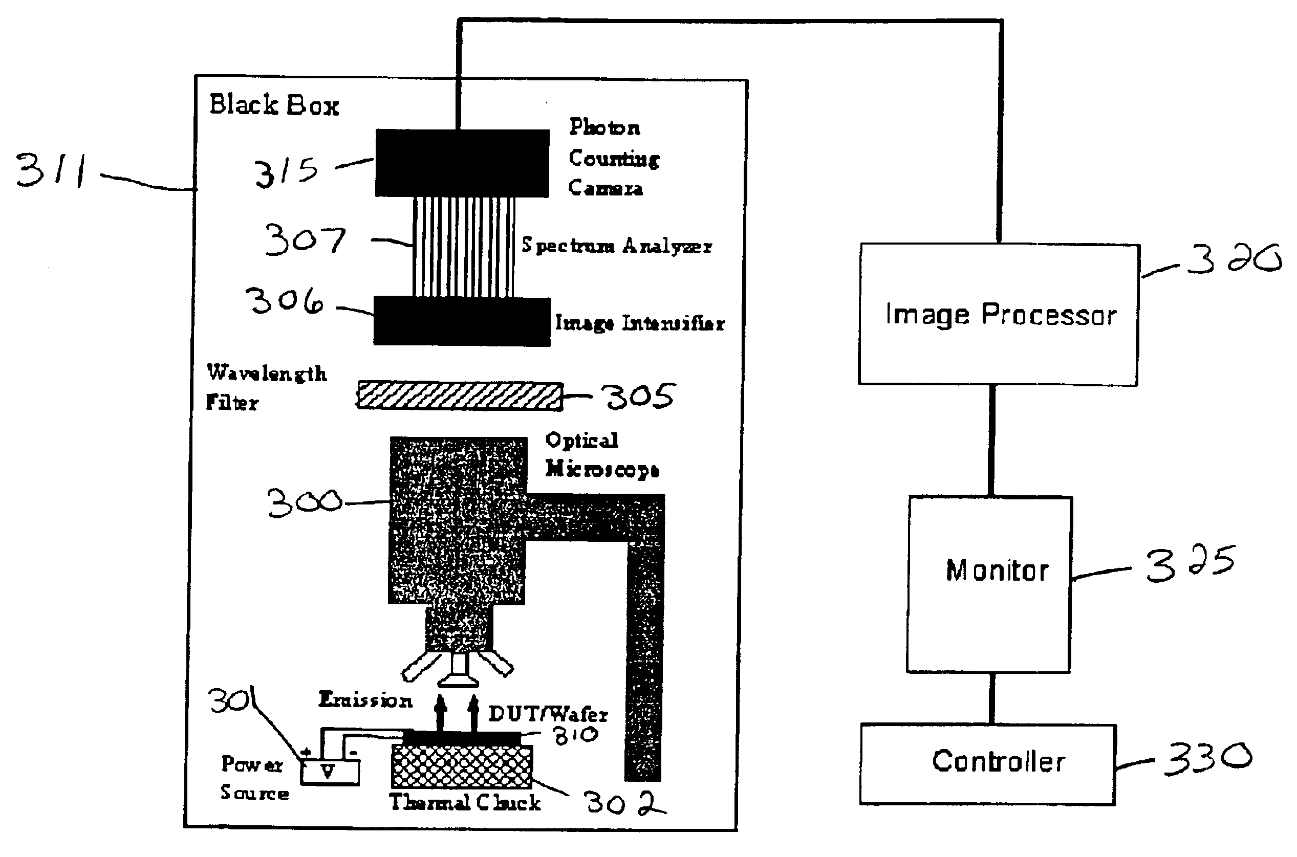
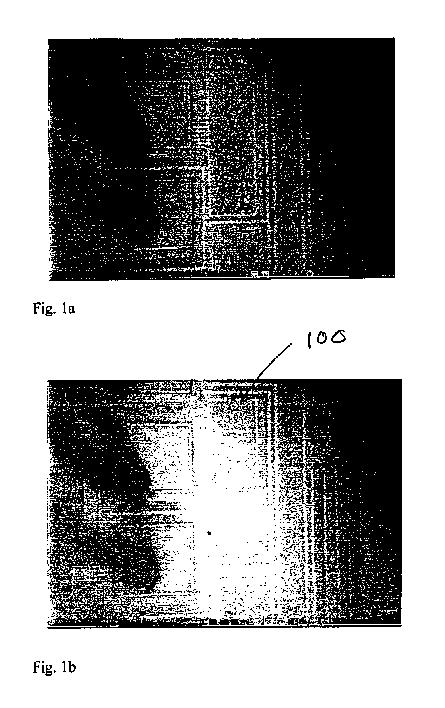
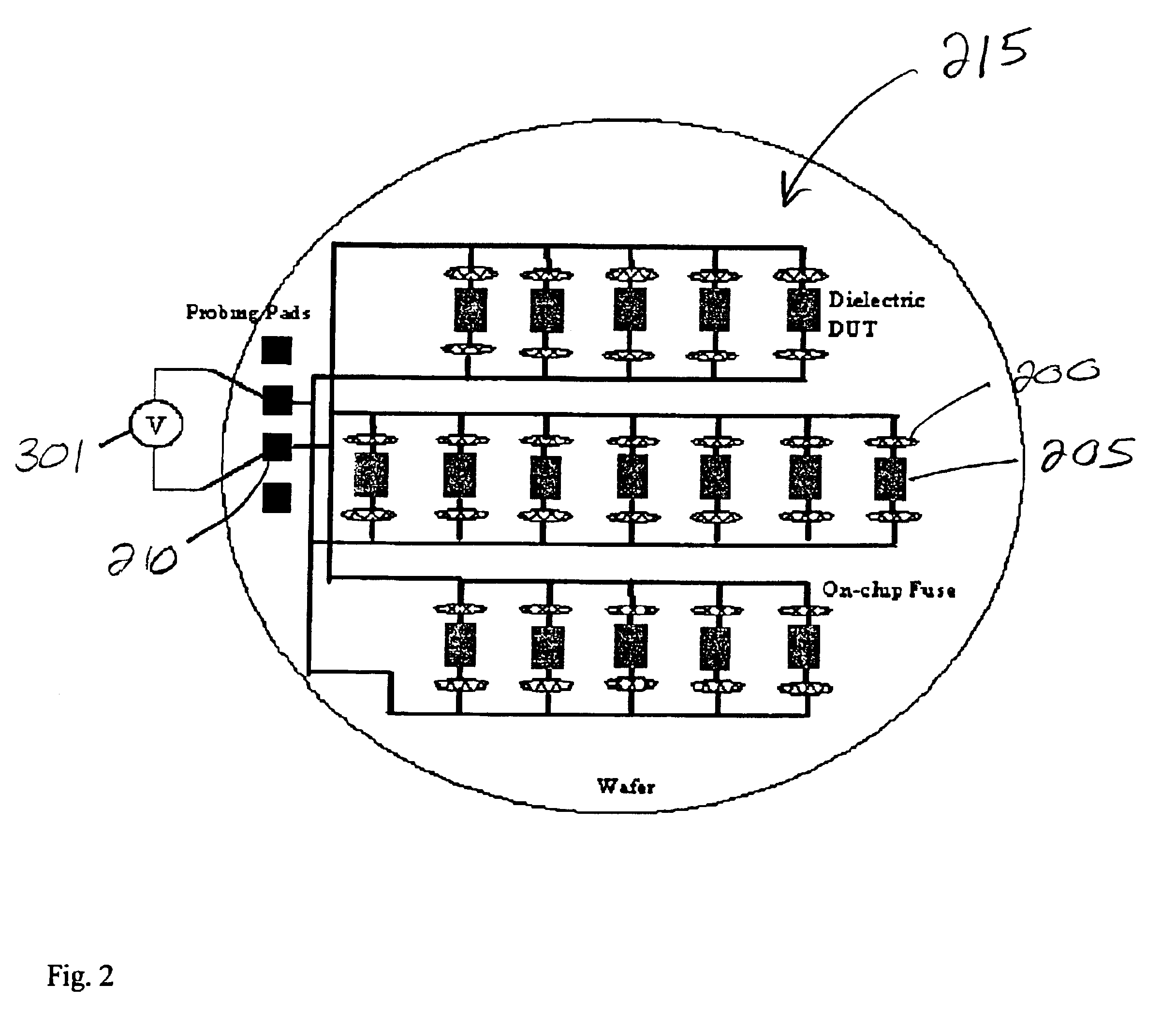
The invention uses an optical emission microscopy technique with spectral resolution capabilities for real-time monitoring of the oxide wear out and breakdown process of many devices across the whole wafer simultaneously. With the real-time image recording, the time of oxide breakdown, the location of breakdown, the change of the light emission intensity during the stress, and the spectral response of the emitted light from breakdown spots provide extensive information regarding oxide wear-out and breakdown physics. With inventive test site design, only one voltage source (for regular constant voltage stress) or current source (for regular constant current stress) is required for stressing and monitoring many devices across the wafer simultaneously. The invention utilizes a simple and reliable setup with very limited hardware to achieve fast massively parallel stress for oxide breakdown at the wafer level.

It is possible for good devices to emit light as well as failing devices, depe...


PUM


Abstract

A method and structure tests devices on a wafer by applying an electrical bias to the devices and simultaneously monitoring emitted light from all of the devices. The emitted light indicates locations of defective devices and records time-based images of the emitted light across the wafer.

Description

1. Field of the InventionThe present invention generally relates to a system and method for testing the reliability of integrated circuit structures and more particularly to an improved wafer-level dielectric reliability test system and method utilizing the contactless detection of optical signal (photon emission) instead of conventional electrical signals such as voltage, current, and resistance to determine time dependent device failure for large-scale reliability evaluations. The invention isolates defective devices through the use of fuses with a specific test structure design allowing the remaining devices to be continuously emission tested.2. Description of the Related ArtReliability evaluation processes such as time-dependent dielectric breakdown stress testing are required for semiconductor manufacturing processes. The purpose of this testing is to ensure qualified technology and to prevent defective and less reliable chips from reaching the user. Current processes heavily u...

Claims


Application Information

Patent Timeline
Patent Type & Authority Patents(United States)
IPC IPC(8): G01R31/28G01R31/311G01R31/12
CPCG01R31/1263G01R31/311
Inventor AITREN, JOHN M.CHEN, FENCONDON, KEVIN L.DIONNE, MARK F.NUTTALL, GREGORY E.
Owner GLOBALFOUNDRIES U S INC
Why Eureka
Try Eureka