Semiconductor package and package stack made thereof

a technology of semiconductors and packages, applied in the direction of semiconductor devices, semiconductor/solid-state device details, electrical devices, etc., can solve the problems of increasing the density of chip integration, high cost, and technical limitations

Inactive Publication Date: 2004-11-02
SAMSUNG ELECTRONICS CO LTD
View PDF8 Cites 42 Cited by
  • Summary
  • Abstract
  • Description
  • Claims
  • Application Information

AI Technical Summary

Problems solved by technology

However, increasing the density of integration of chips may be expensive and have technical limitations.

Method used


Image

  • Semiconductor package and package stack made thereof
  • Semiconductor package and package stack made thereof
  • Semiconductor package and package stack made thereof

Examples


Embodiment Construction

Exemplary embodiments of the invention will be described below with reference to the accompanying drawings.

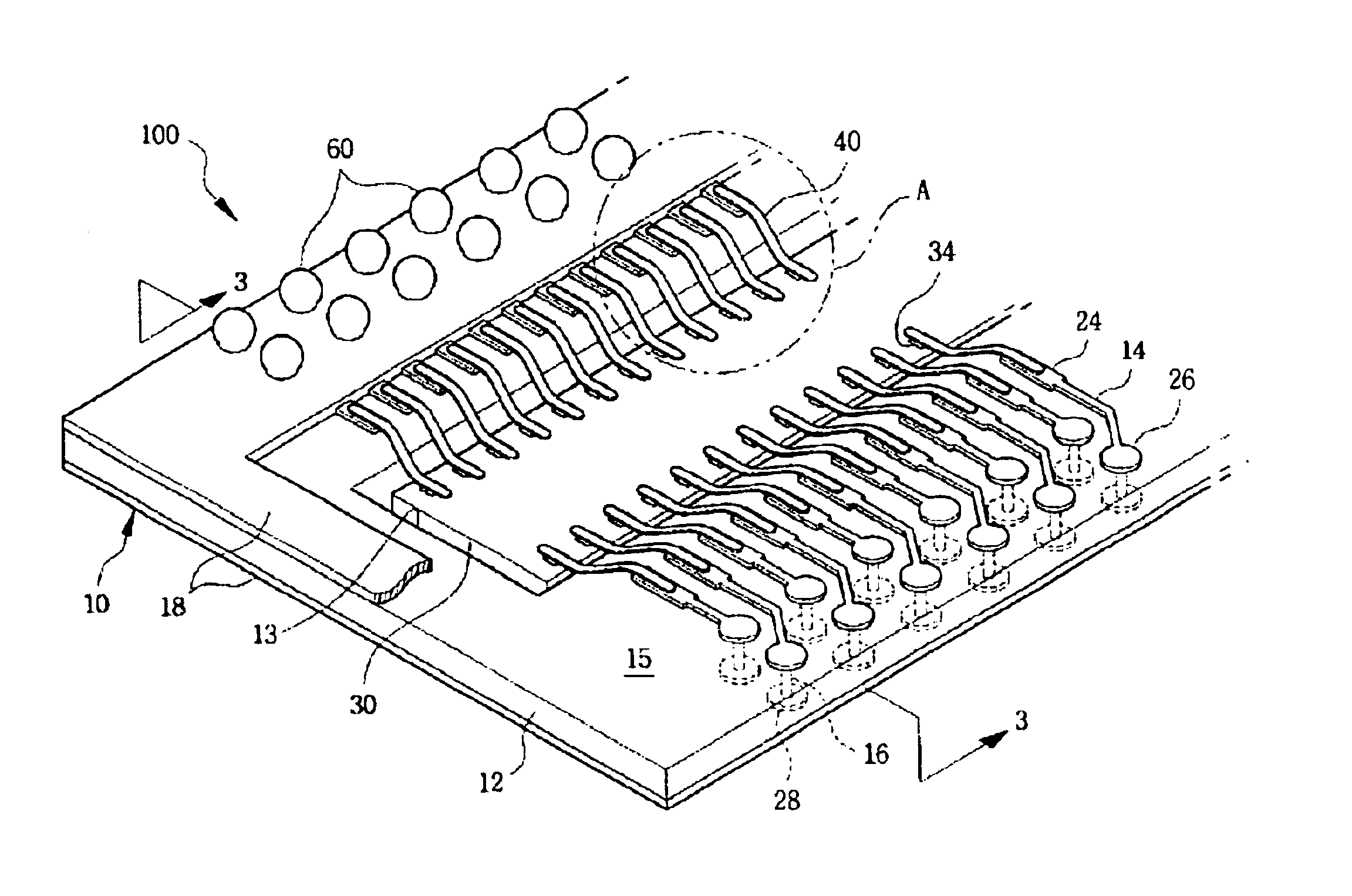
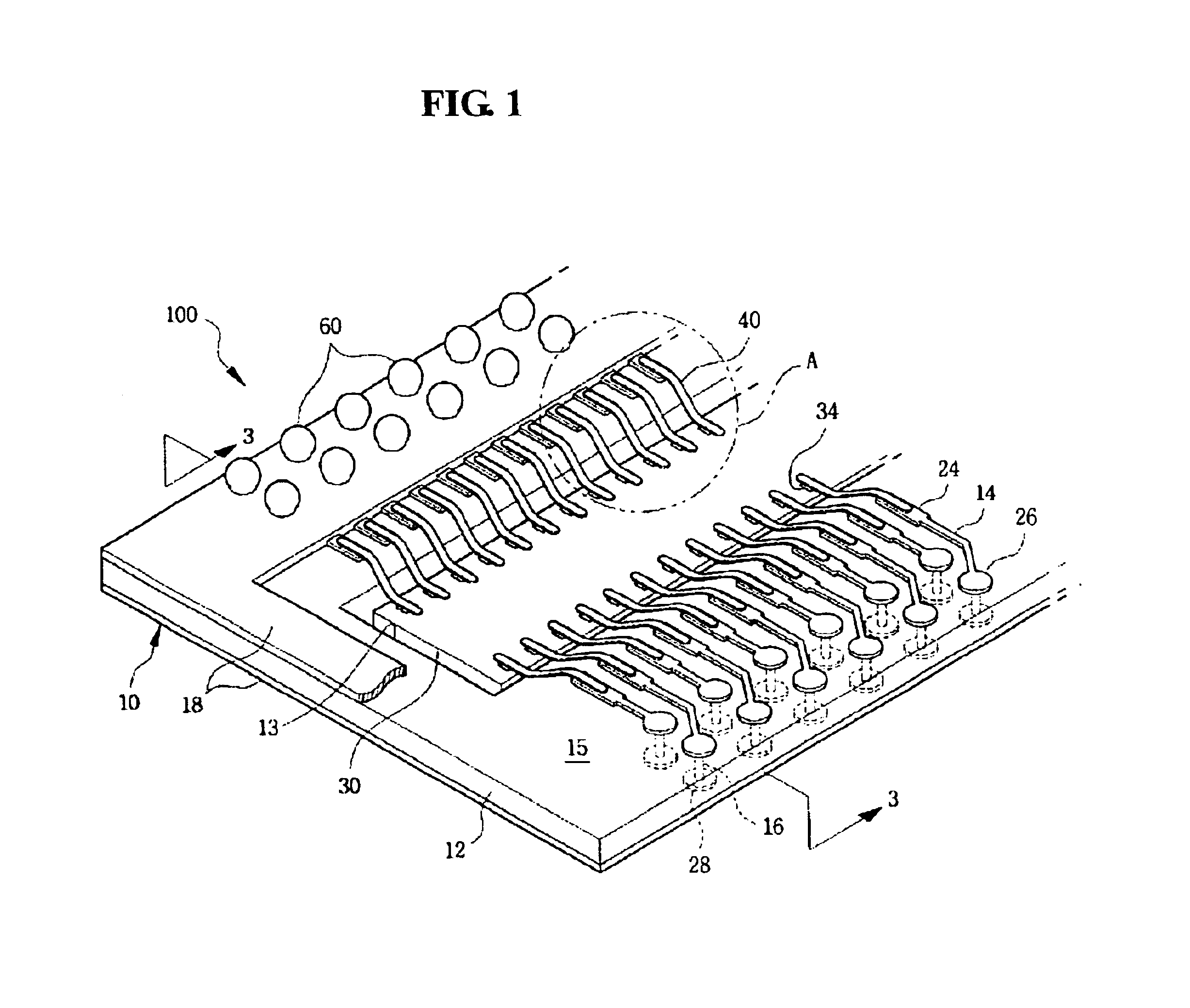
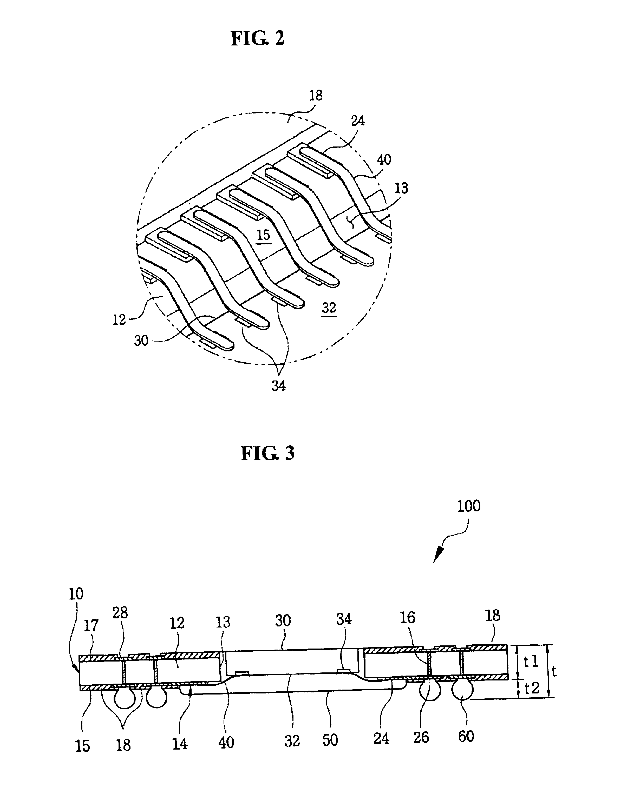
The structure of a semiconductor package (100) according to an exemplary embodiment of the invention will be described referring to FIG. 1.about.FIG. 3. In FIG. 1 and FIG. 2, an encapsulation part (50) shown in FIG. 3 is not shown for convenience of explanation.

Referring to FIG. 1.about.FIG. 3, a semiconductor package according to an exemplary embodiment of the invention comprises a semiconductor chip (30), a board (10) and an electrical connector between the chip (30) and the board (10).

More specifically, the board (10) may comprise an upper surface (17), a lower surface (15) and an aperture (13) formed in a central region of the board (10). In FIG. 1, the package (100) is illustrated with the lower surface (15) of the board (10) upward.

In other exemplary embodiments, the board (10) may contain more than one aperture (13) and the aperture or apertures (13) may be located anywh...


PUM


Abstract

A semiconductor package comprises a board, a plurality of solder bump pads, a plurality of board pads, a plurality of distribution patterns, a plurality of contact pads, at least one chip, a plurality of bonding wire, an encapsulation part and a plurality of solder bumps. In order to reduce the height of the loop of the bonding wires for connecting the bonding pad on the semiconductor chip to the board pads on the board, the ends of the bonding wires are connected to the bonding pads and board pads respectively by wedge bonding. Thus, a very thin package can be obtained. In addition, a thin package stack can be obtained by stacking the very thin packages.

Description

1. Field of the InventionThe present invention relates to a semiconductor package and a package stack made thereof.2. Description of the Prior ArtThe electronic industry continues to seek products that are lighter, faster, smaller, multi-functional, more reliable and more cost-effective. In order to meet the requirement of the electronic industry, circuit chips should be more highly integrated.However, increasing the density of integration of chips may be expensive and have technical limitations. Therefore, three-dimensional (3-D) type semiconductor packaging techniques have been developed and used. In general, package stacks made by stacking a plurality of packages and stacked chip packages made by stacking a plurality of chips in a package have been used.Package stacks may be manufactured by stacking packages that have already passed the necessary tests for their functions. Therefore, the yields and reliability of these package stacks may be higher than those stacked chip packages...

Claims


Application Information

Patent Timeline
Patent Type & Authority Patents(United States)
IPC IPC(8): H01L23/13H01L23/28H01L23/31H01L23/48H01L23/12H01L23/498H01L25/10H01L21/60H01L21/607
CPCH01L23/13H01L23/3128H01L25/105H01L24/85H01L23/49816H01L2224/85099H01L2225/1058H01L2225/1035H01L2924/014H01L2924/00014H01L24/48H01L2924/18165H01L2924/1532H01L2924/15311H01L2924/1517H01L2924/15153H01L2924/01079H01L2924/01078H01L2924/01029H01L2924/01013H01L2924/01006H01L2224/85205H01L2224/48472H01L2224/48091H01L2224/45147H01L2224/45144H01L2224/45124H01L24/45H01L2224/78H01L2924/00H01L2924/181H01L2224/05599H01L2224/85399H01L2224/05554H01L2224/45099H01L2924/00012H01L23/28
Inventor KIM, JIN-HOOH, SE-YONG
Owner SAMSUNG ELECTRONICS CO LTD
Why Eureka
Try Eureka