Correction of spacing violations between dummy geometries and wide class objects of design geometries

a geometries and wide class technology, applied in the field of electronic circuits, can solve the problems of complicated and time-consuming process of electronic circuit design, detailed design layout, and high design effort for detailed design layou

Inactive Publication Date: 2004-11-09
ORACLE INT CORP
View PDF9 Cites 8 Cited by
  • Summary
  • Abstract
  • Description
  • Claims
  • Application Information

AI Technical Summary

Problems solved by technology

Design of an electronic circuit, for example, an integrated circuit (IC), is a complicated and time consuming process. FIG. 1 illustrates a typical design flow 100 of an integrated circuit device from conception through the generation of a fabrication ready design layout.
The detailed design layout requires a very intensive and time-consuming design effort and is typically performed utilizing specialized computer aided design (CAD) or Electronic Design Automation (EDA) tools.
DRC is a time-consuming iterative process that often requires manual manipulation and interaction by the designer.
Creation of a design layout and performing DRC become critical time consuming processes.

Method used


Image

  • Correction of spacing violations between dummy geometries and wide class objects of design geometries
  • Correction of spacing violations between dummy geometries and wide class objects of design geometries
  • Correction of spacing violations between dummy geometries and wide class objects of design geometries

Examples


Embodiment Construction

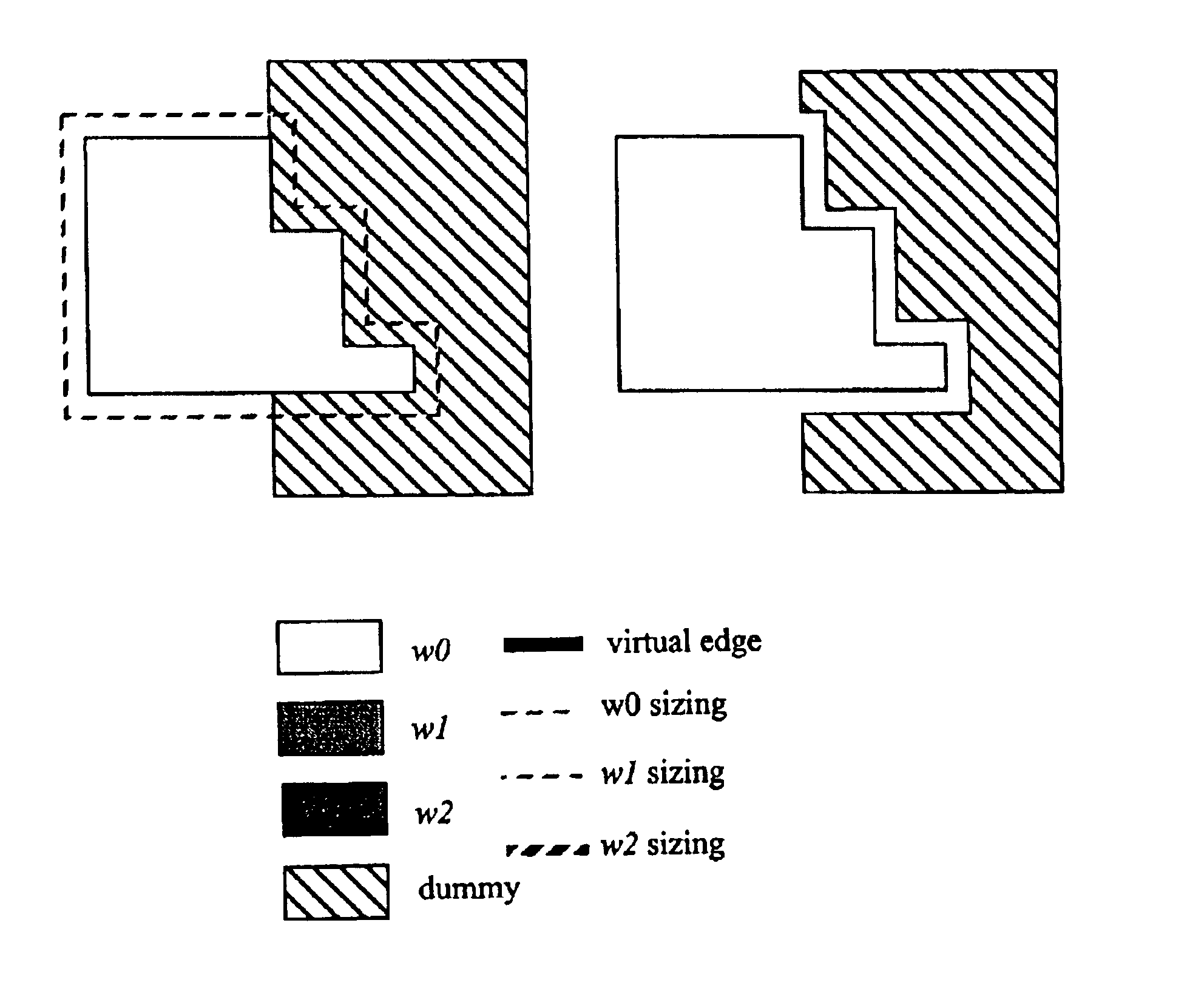
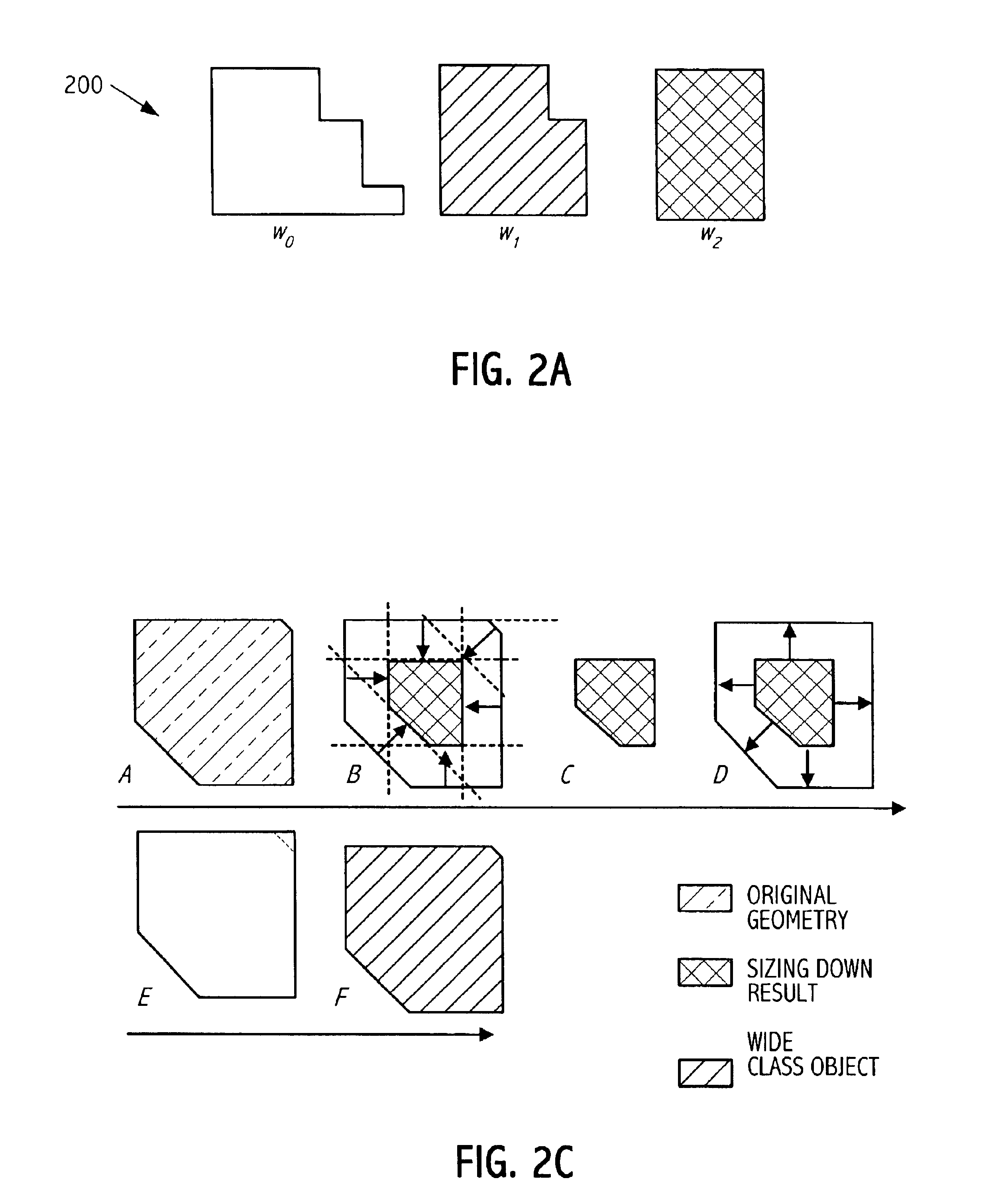
FIGS. 2A-2E illustrate various geometries and their features as utilized by some embodiments of the present invention. A geometry can be metal or polysilicon, or other such material. As illustrated in FIG. 2A, a geometry 200 can be of irregular shape. The irregular shape of a geometry can be due to reshaping of the geometry to conform to design rules, allowance for via placement, and other such design reasons.

Design rules are typically different for different sized geometries. For example, larger geometries require a larger amount of space between other geometries than is required by smaller geometries. Because the design rules are typically different for different sized geometries, geometries are often classified according to size. Classifying a shape such as geometry 200 can lead to several options. For example, geometry 200 can be classified according to its widest edge, applying worst case spacing requirements. Applying the worst case spacing requirements is not a desirable clas...


PUM


Abstract

Automated techniques to correct certain rule violations with respect to non-design geometries are used, simplifying and automating the design layout of an electronic circuit, whether embodied as a design encoding or as a fabricated electronic circuit. Correcting a minimum spacing rule violation between a non-design geometry and one or more wide class objects of a design geometry is accomplished by deducting an enlarged wide class object of the design geometry from the non-design geometry; wherein the enlarged wide class object is formed by enlarging a wide class object of the design geometry at one or more non-virtual edges of the wide class object but not at one or more virtual edges of the wide class object, wherein the wide class object of the design geometry has at least one virtual edge.

Description

1. Field of the InventionThis invention relates to electronic circuits and more particularly to complex computer aided design layout and design rule verification of a design layout of, for example, an integrated circuit (IC) device or printed wiring board, in preparation for fabrication.2. Description of the Related ArtDesign of an electronic circuit, for example, an integrated circuit (IC), is a complicated and time consuming process. FIG. 1 illustrates a typical design flow 100 of an integrated circuit device from conception through the generation of a fabrication ready design layout. Generally, design flow 100 commences with defining the design specifications or requirements, such as required functionality and timing, step 102. The requirements of the design are implemented, for example, as a net-list or electronic circuit description, step 104. The implementation can be performed by, for example, schematic capture (drawing the design with a computer aided design tool) or more ty...

Claims


Application Information

Patent Timeline
Patent Type & Authority Patents(United States)
IPC IPC(8): G06F17/50
CPCG06F17/5068G06F30/39
Inventor LI, MU-JING
Owner ORACLE INT CORP
Why Eureka
Try Eureka