Method of purging wafer receiving jig, wafer transfer device, and method of manufacturing semiconductor device

a technology of wafer receiving jig and wafer transfer device, which is applied in the direction of transportation and packaging, drying machines, light and heating equipment, etc., can solve the problem of long time required to fill the inside of the foup with inert gas

Inactive Publication Date: 2005-03-15
TRECENTI TECHNOLOGIES INC
View PDF5 Cites 167 Cited by
  • Summary
  • Abstract
  • Description
  • Claims
  • Application Information

AI Technical Summary

Problems solved by technology

However, the atmosphere in the FOUP is pushed by the inert gas introduced from the gas supply passage to be flowed toward the exhaust passage, so there is presented a problem tha...

Method used


Image

  • Method of purging wafer receiving jig, wafer transfer device, and method of manufacturing semiconductor device
  • Method of purging wafer receiving jig, wafer transfer device, and method of manufacturing semiconductor device
  • Method of purging wafer receiving jig, wafer transfer device, and method of manufacturing semiconductor device

Examples


embodiment 1

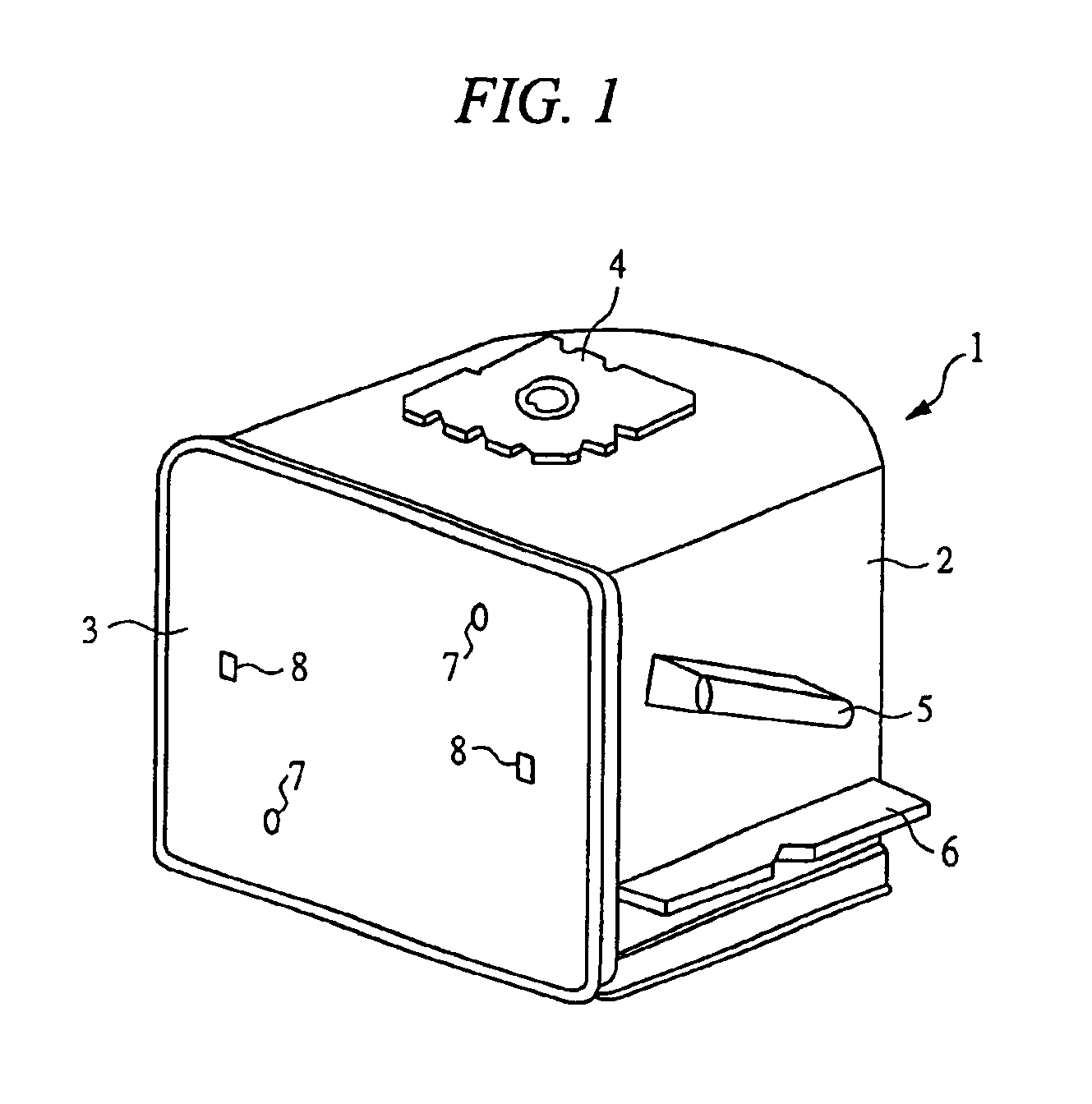
FIG. 1 is a perspective view showing one example of the external appearance construction of a FOUP of embodiment 1 of the invention.

A FOUP 1 is constructed on a shell 2 which is a part for holding a semiconductor wafer and a door 3 which is a part for opening or closing the shell 2. A top flange 4 gripped by a robot at the time of automatically transferring the FOUP 1 by the robot is provided on the top of the shell 2. A manual handle 5 and a side rail 6 are provided on the side of the shell 2. The manual handle 5 is used, for example, at the time of lifting up the FOUP 1 by hand and the side rail 6 is used, for example, at the time of scooping up the FOUP 1 by the robot. Moreover, a breathing filter (not shown) is provided on the bottom of the shell 2.

Further, registration pin holes 7 for positioning the FOUP 1 and latch key holes 8 for opening the door 3 by the robot are formed in the outside of the door 3.

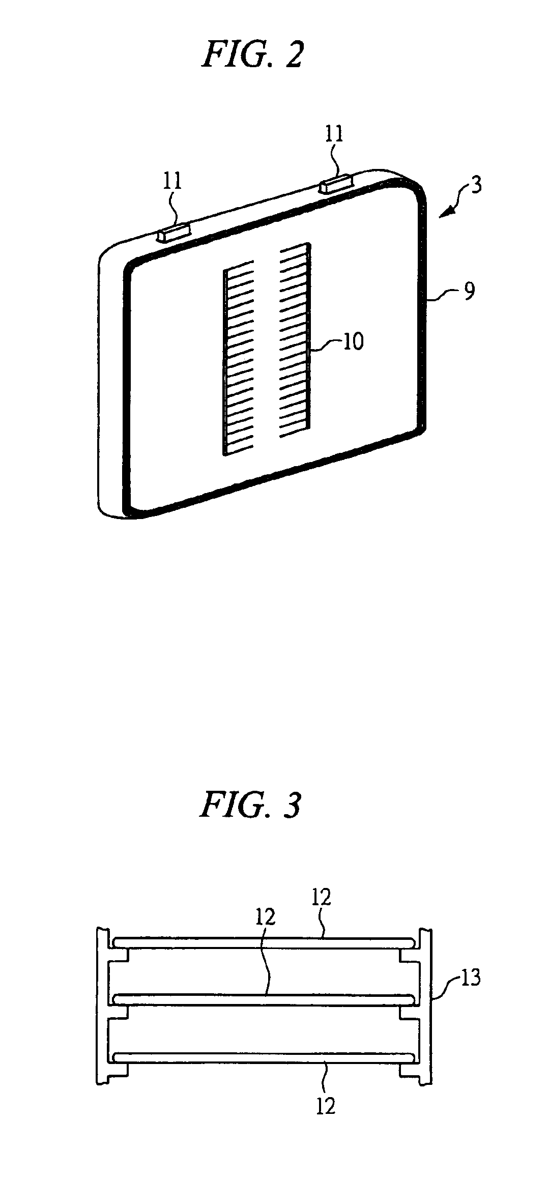
FIG. 2 is a perspective view showing one example of the inside construction...

embodiment 2

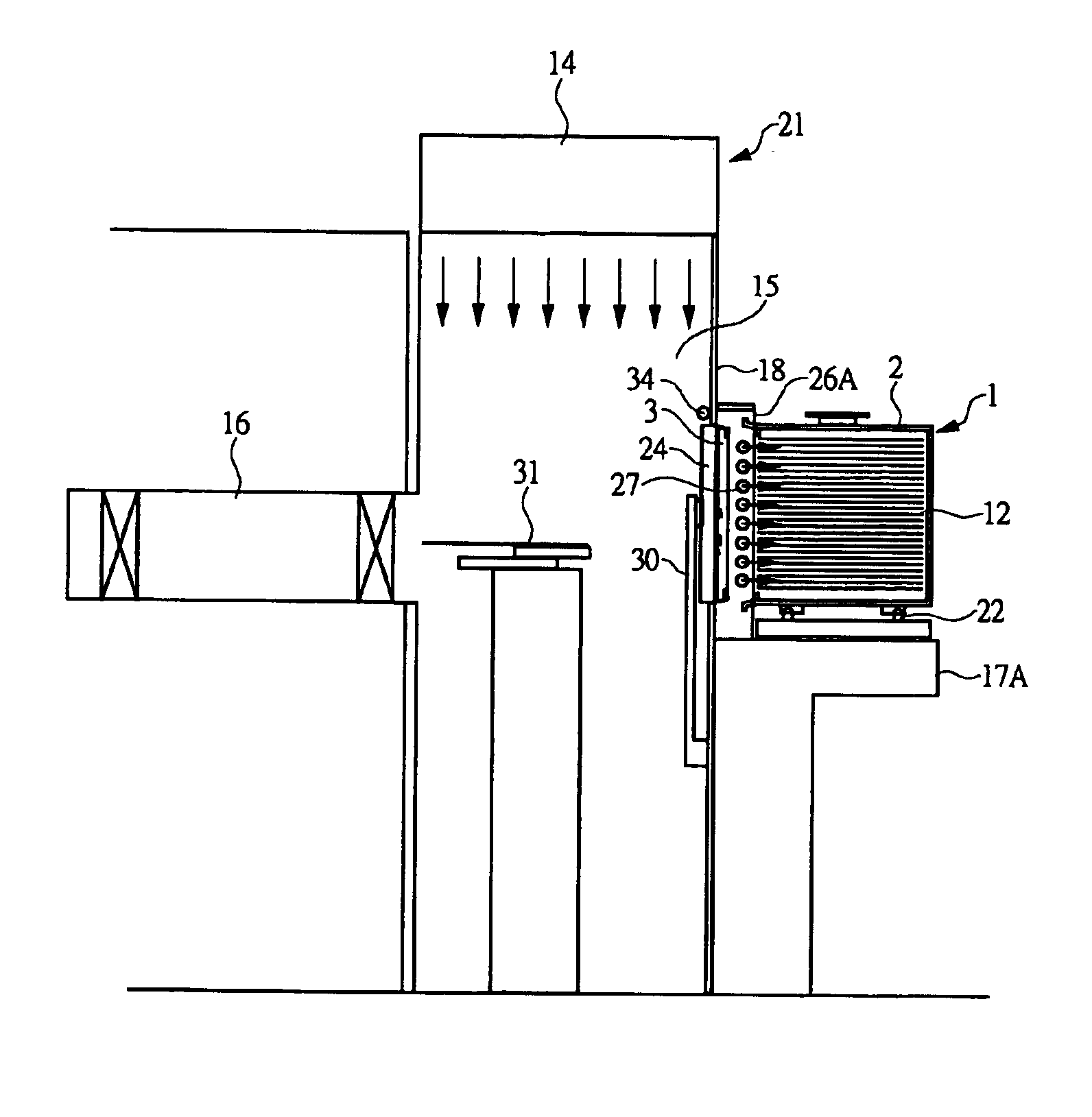
A method of purging a FOUP which is embodiment 2 of the invention will be described by the use of a construction view, shown in FIG. 16, of a semiconductor manufacturing device and the FOUP placed on the loading port.

As is the case with the above embodiment 1, a semiconductor manufacturing device 33 is provided with the mini environment 15 having the FFU 14 and the load / lock 16 and the loading port 17. The degree of cleanliness in the mini environment 15 separated from the outside by the box surface 18 is, for example, Class 1 and the degree of cleanliness of the outside is, for example, Class 1000. Further, a gas introduction pipe 34 capable of supplying purge gas is provided above the FIMS door 24.

As is the case with the above embodiment 1, the FOUP1 having predetermines pieces of semiconductor wafers 12 received therein is transferred to the loading port 17 of the semiconductor manufacturing device 33. Then, the FOUP 1 is moved forward to engage the door 3 of the FOUP 1 with the ...

embodiment 3

The structures of the FOUP and the semiconductor manufacturing device of this embodiment 3 are nearly similar to those of the FOUPs and the semiconductor manufacturing devices (see FIG. 1 to FIG. 16) of the above embodiments 1 and 2.

A method of purging the FOUP which is embodiment 3 of the invention will be described with reference to FIG. 17 to FIG. 25. FIG. 17 is a construction view showing the FOUP placed on the base of the semiconductor manufacturing device. FIG. 18 to FIG. 21 are construction views showing the semiconductor manufacturing device and the FOUP placed on the base of the semiconductor manufacturing device. FIG. 22 to FIG. 25 are schematic views showing the flow of the purge gas.

In this respect, in the semiconductor manufacturing device shown in FIG. 18 to FIG. 21, the mini environment 15 provided with the FFU 14, the load / lock 16 and a base 17A are shown, whereas the processing chamber and the exhaust system are omitted.

First, the FOUP 1 having predetermined pieces ...


PUM


Abstract

A FOUP having semiconductor wafers received therein is transferred to a loading port and then the door of the FOUP is fixed and removed by a FIMS door and then the semiconductor wafers are taken out of the shell of the FOUP and then a predetermined manufacturing processing is performed to the semiconductor wafers. After performing the manufacturing processing, the semiconductor wafers are returned into the shell and the FIMS door is returned to a closed position and the shell is retracted about 50 mm to 65 mm to form a gap between the FIMS door and the shell. Then, purge gas is introduced from a gas introduction pipe arranged above the loading port on the left and right sides in a slanting forward direction of the FIMS door into the shell to replace the atmosphere in the shell with the purge gas.

Description

TECHNICAL FIELD OF THE INVENTIONThe present invention relates to a technology for manufacturing a semiconductor device and, in particular, to a technology effectively applied to a method of purging a wafer receiving jig for storing or transferring a semiconductor wafer of 300 mm in diameter at the time of manufacturing a semiconductor, a loading port for opening or closing the wafer receiving jig, and a method of manufacturing a semiconductor device.BACKGROUND OF THE INVENTIONIn order to store or transfer a semiconductor wafer of 300 mm in diameter at the time of manufacturing a semiconductor, for example, a side door integrated wafer receiving jig is used which is called a front opening unified pod (FOUP) having an opening door in a front portion through which the semiconductor wafer is inserted into or taken out of the jig. The FOUP is constructed of a shell which is a holding part for receiving the semiconductor wafer and a door which is a part for opening or closing the shell. T...

Claims


Application Information

Patent Timeline
IPC IPC(8): H01L21/00H01L21/677H01L21/68H01L21/67H01L21/673
CPCH01L21/67017H01L21/68H01L21/67772
Inventor TOKUNAGA, KENJI
Owner TRECENTI TECHNOLOGIES INC
Why Eureka
Try Eureka