Double-sided extended drain field effect transistor, and integrated overvoltage and reverse voltage protection circuit that uses the same

a technology of drain field effect transistor and drain field effect, which is applied in the direction of instruments, semiconductor devices, electrical apparatus, etc., can solve the problems of limitless variety of applications, circuitry is only designed to operate, and circuitry is limited to electrical circuitry

Inactive Publication Date: 2005-03-15
SEMICON COMPONENTS IND LLC
View PDF17 Cites 7 Cited by
  • Summary
  • Abstract
  • Description
  • Claims
  • Application Information

AI Technical Summary

Benefits of technology

The use of double-sided extended drain field effect transistors permits a less complex design for the protection circuit that thereby reduces layout complexity and size. Furthermore, the voltage regulator and reverse voltage protection circuit are integrated to allow for more convenient use in applications in which both overvoltage and reverse voltage conditions may apply. Furthermore, the circuit may be fabricated using standard CMOS processes and does not require components external to the chip to operate.

Problems solved by technology

Electrical circuits are in widespread use with a practically limitless variety of applications.
Nevertheless, there are limits to electrical circuitry.
One limit is that circuitry is only designed to operate with certain applied electrical voltages.
If those supplied electrical voltages should vary from the designed electrical voltage conditions, circuitry may be damaged or destroyed.
Such damage or destruction is most often undesired and may often even be unacceptable.
Some protection circuits substantially stop any power at all from being delivered to the load circuit if anomalous voltage conditions are applied to the protection circuit.
Also, sometimes the battery may be inadvertently connected in reverse, in which case the load circuitry may be subject to applied electrical voltages that have opposite polarity as compared to the designed applied voltages.
Without protection, this may result in normally reverse-biased PN semiconductor junctions to be forward-biased, which can devastate semiconductor-based circuitry.
In addition, many protection circuits use depletion mode transistors (normally on) or devices such as bipolar transistors, Schottky diodes, or other types of devices that also may not be available in many standard Complementary Metal-Oxide-Silicon (CMOS) processes.
Even if available, the process complexity involved with fabricating such devices is higher.
Thus, the presence of such devices increases the cost of the circuit.
Also, such devices may significantly increase the voltage drop across the protection circuit even if the applied supply voltages are within the designed tolerances of the load circuit.
Many protection circuits also may require oscillators, charge pumps, DC-DC converters, or other complex circuits that may significantly increase the cost, size and power dissipation of the protection circuit.

Method used


Image

  • Double-sided extended drain field effect transistor, and integrated overvoltage and reverse voltage protection circuit that uses the same
  • Double-sided extended drain field effect transistor, and integrated overvoltage and reverse voltage protection circuit that uses the same
  • Double-sided extended drain field effect transistor, and integrated overvoltage and reverse voltage protection circuit that uses the same

Examples


Embodiment Construction

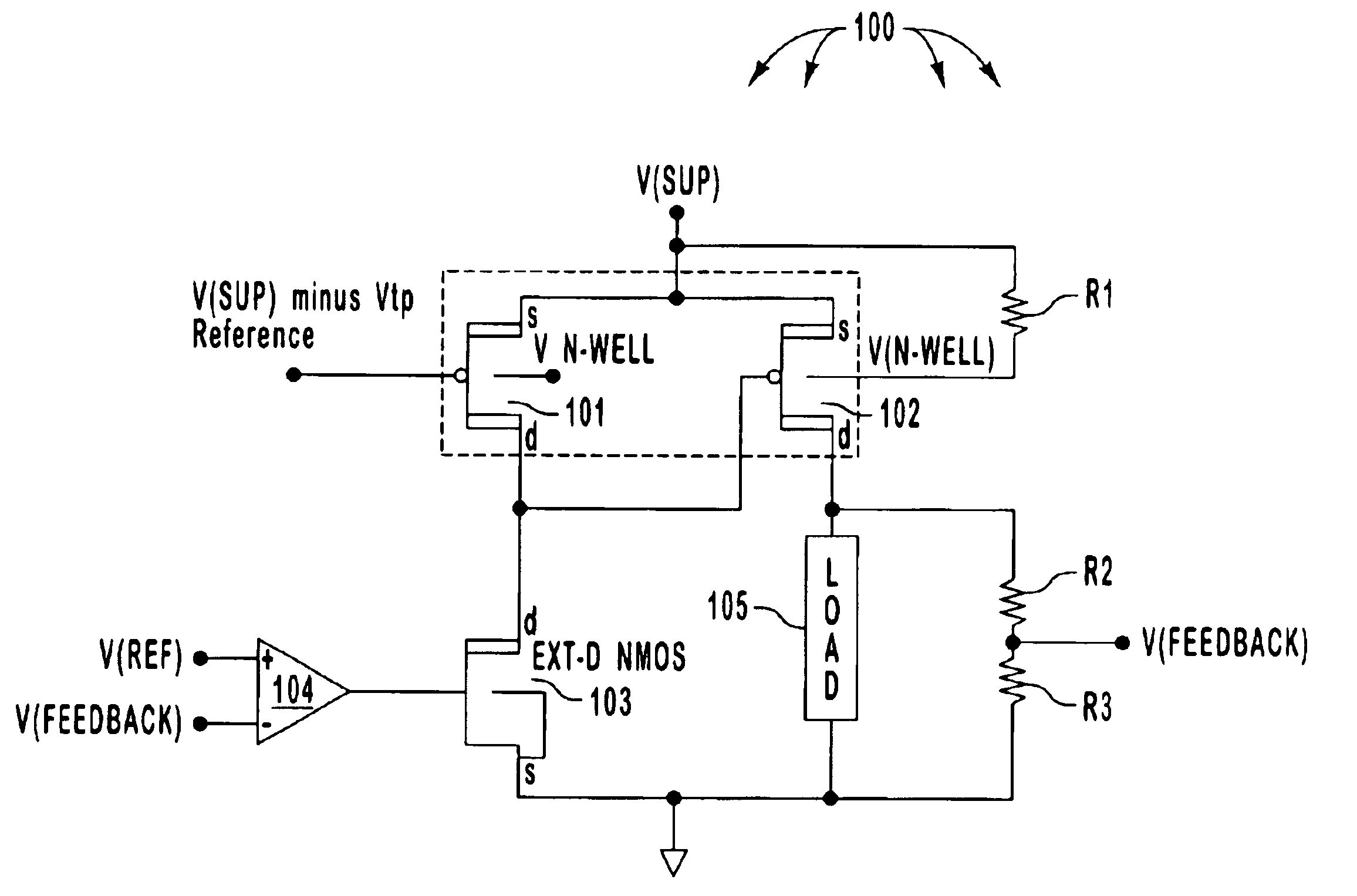
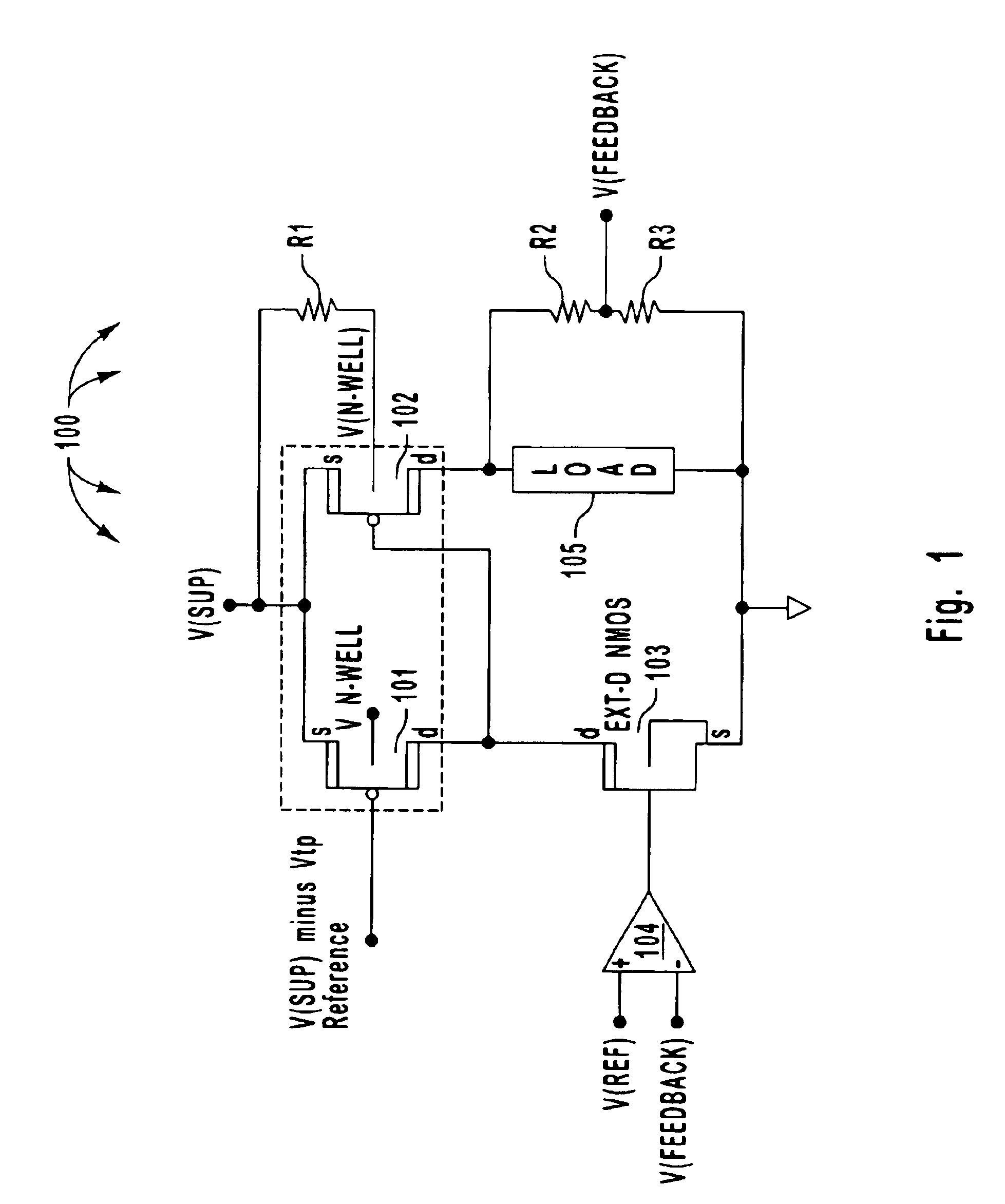
The present invention relates to an integrated overvoltage and reverse voltage protection circuit that implements double-sided extended drain field effect transistors to thereby effect a design that occupies relatively little area and that may be implemented using standard CMOS processes.

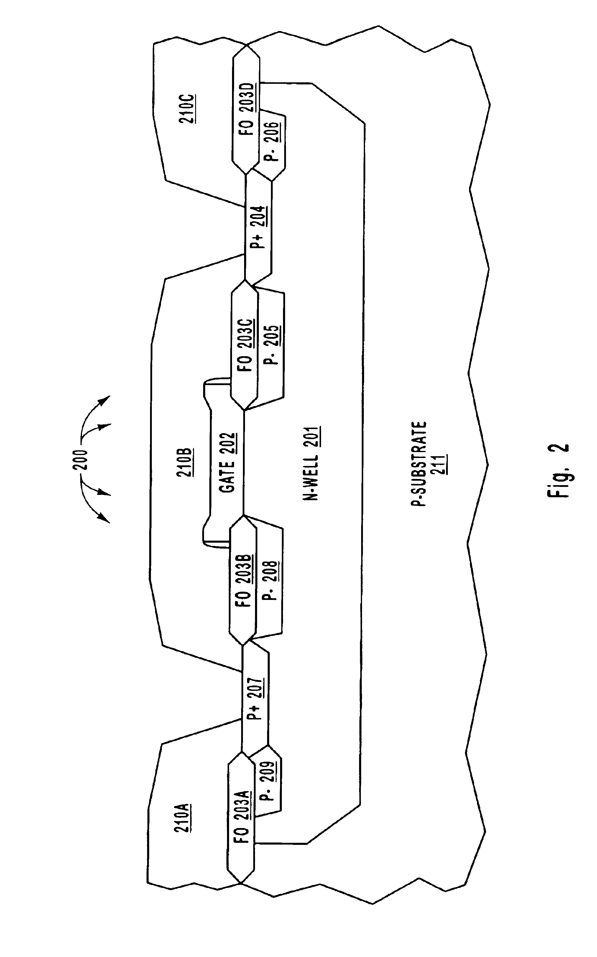
FIG. 1 illustrates an integrated voltage regulator and reverse voltage protection circuit 100 in accordance with the principles of the present invention. The circuit 100 includes two p-channel double-sided extended drain field effect transistors 101 and 102. In this description and in the claims, a “double-sided extended drain field effect transistor” is any field effect transistor in which there is a RESURF region between the drain terminal and the channel region, and another RESURF region between the source terminal and the channel region. “RESURF” is short for “REduced SURface Field”. The circuit 100 also includes an n-channel extended drain field effect transistor 103. The n-channel extended dra...


PUM


Abstract

An integrated overvoltage and reverse voltage protection circuit that includes two p-channel double-sided extended drain transistors coupled to a high voltage source, each having their n-well coupled through a resistor to the high voltage source. For voltage regulation, a voltage divider is coupled in series with a first of these transistors, while the drain of the second transistor is coupled to the gate of the first transistor. For voltage blocking, the voltage divider may span the entire supply voltage. An n-channel transistor couples the second p-channel transistor to a low voltage source. A middle node in the voltage divider is coupled to one input of a comparator, with a reference voltage coupled to the second input. The comparator output drives the gate terminal of the n-channel transistor. A load to be protected may be disposed in parallel with the voltage divider.

Description

BACKGROUND OF THE INVENTION1. The Field of the InventionThe present invention relates generally to extended drain field effect transistors and electrical power protection circuits. More specifically, the present invention relates to double-sided extended drain field effect transistors and an integrated overvoltage and reverse voltage protection circuit that uses double-sided extended drain field effect transistors.2. Background and Related ArtElectrical circuits are in widespread use with a practically limitless variety of applications. Innovation in circuit design has changed the very way we live and work. Nevertheless, there are limits to electrical circuitry. One limit is that circuitry is only designed to operate with certain applied electrical voltages. If those supplied electrical voltages should vary from the designed electrical voltage conditions, circuitry may be damaged or destroyed. Such damage or destruction is most often undesired and may often even be unacceptable. Acc...

Claims


Application Information

Patent Timeline
Patent Type & Authority Patents(United States)
IPC IPC(8): H01L27/02
CPCH01L27/0266
Inventor SCOTT, GREGLARAIA, J. MARCOS
Owner SEMICON COMPONENTS IND LLC
Why Eureka
Try Eureka