Drive circuit to be used in active matrix type light-emitting element array
a technology of drive circuits and light-emitting elements, which is applied in the direction of electric digital data processing, instruments, computing, etc., can solve the problems of unstable display performance of display devices, unfavorable image display, and complex drive control systems, and achieve excellent gray-scale and high quality
- Summary
- Abstract
- Description
- Claims
- Application Information
AI Technical Summary
Benefits of technology
Problems solved by technology
Method used
Image

Examples
embodiment 1
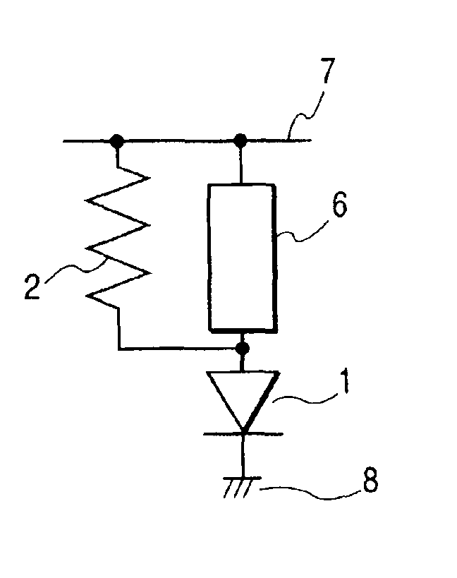
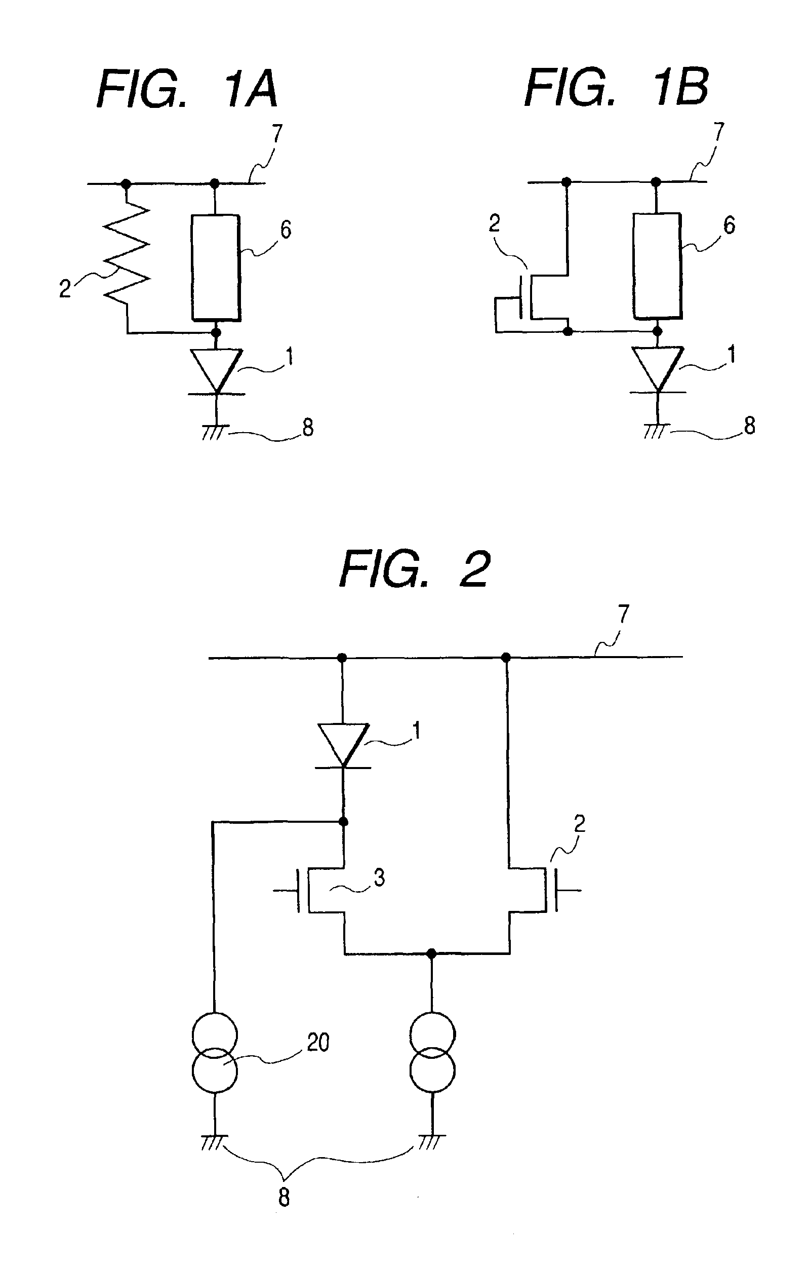
FIGS. 1A and 1B are circuit diagrams of two alternatives of the first embodiment of drive circuit to be used in an active matrix type light-emitting element array according to the invention. In FIG. 1A, a resistance element 2 is connected between a power supply line 7 and a light-emitting element 1, whereas the resistance element is replaced by a thin film transistor (TFT) in FIG. 1B.
The drive circuit of this embodiment is so designed as to be used in an active matrix type light-emitting element array comprising scan lines and signal lines (not shown in FIGS. 1A and 1B) arranged to form a matrix on a substrate and unit pixels arranged near the respective crossings of the scan lines and the signal lines, each unit pixel having a resistance element 2, a picture signal current supply circuit 6 and a light-emitting element 1 adapted to be caused to emit light by the picture signal current.
The light-emitting element 1 is realized by using an organic EL element that is made of a plurality...
embodiment 2
FIG. 2 is a circuit diagram of the second embodiment of the invention showing the pixel circuit related to it. This embodiment is additionally provided with a constant current circuit 20 for causing a bias current to flow through an organic EL element 1 for high speed operation. The first electrode and the second electrode of the constant current circuit 20 are connected respectively to the cathode of the organic EL element 1 and a grounding line 8. The constant current circuit 20 and the organic EL element 1 are connected in series between a power supply line 7 and the ground potential 8 and the constant current circuit 20 operates to limit the bias current flowing through the organic EL element to a value that reduces the brightness of emitted light to less than a predetermined level, a fraction of the lowest brightness for example. With this arrangement, the bias current is held to a level lower than that of the electric current that can produce the lowest brightness of emitted l...
embodiment 3
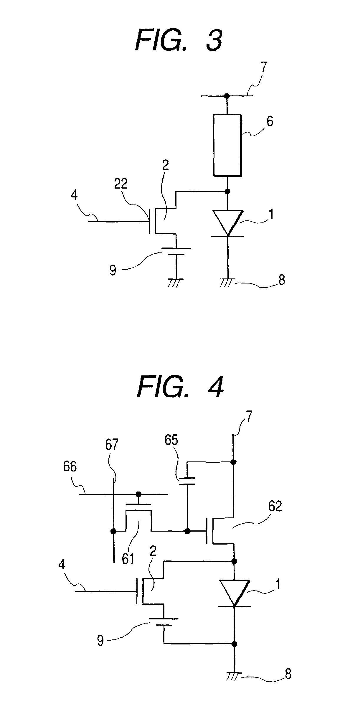
FIG. 3 is a third embodiment of drive circuit to be used in an active matrix type light-emitting element array according to the invention.
The drive circuit of this embodiment is so designed as to be used in an active matrix type light-emitting element array comprising scan lines (not shown) and signal lines 4 arranged to form a matrix on a substrate and unit pixels arranged near the respective crossings of the scan lines and the signal lines, each unit pixel having a picture signal current supply circuit 6 and a light-emitting element 1 adapted to be caused to emit light by the picture signal current.
As shown in FIG. 3, one of the electrodes of the organic EL element 1 is commonly connected to the source electrode of the TFT 2 as viewed from the power supply line 7, while the other electrode of the organic EL element 1 is connected to the ground potential 8 that operates as power source. The drain electrode of the TFT 2 is connected to a reference voltage source 9. The source electr...
PUM
 Abstract
Description
Claims
Application Information
 - R&D Engineer
- R&D Manager
- IP Professional
- Industry Leading Data Capabilities
- Powerful AI technology
- Patent DNA Extraction
Browse by: Latest US Patents, China's latest patents, Technical Efficacy Thesaurus, Application Domain, Technology Topic.
© 2024 PatSnap. All rights reserved.Legal|Privacy policy|Modern Slavery Act Transparency Statement|Sitemap