Electrical circuit conductor inspection

a technology of electrical circuit and conductor, applied in the direction of optically investigating flaws/contamination, instruments, measurement devices, etc., can solve the problem of high production cost of printed circuit boards

Inactive Publication Date: 2005-03-22
ORBOTECH LTD
View PDF51 Cites 17 Cited by
  • Summary
  • Abstract
  • Description
  • Claims
  • Application Information

AI Technical Summary

Benefits of technology

The above and other aspects of the invention will be more fully understood and appreciate...

Problems solved by technology

The production of printed circuit boards is an expensive undertaking, and many extr...

Method used


Image

  • Electrical circuit conductor inspection
  • Electrical circuit conductor inspection
  • Electrical circuit conductor inspection

Examples


Embodiment Construction

Using the above-identified figures, the invention will now be described with respect to various embodiments of the invention. Although many specificities will be mentioned, it must be emphasized that the scope of the invention is not be taken to be that of only the embodiments described herein, but should be construed in accordance with the claims appended below.

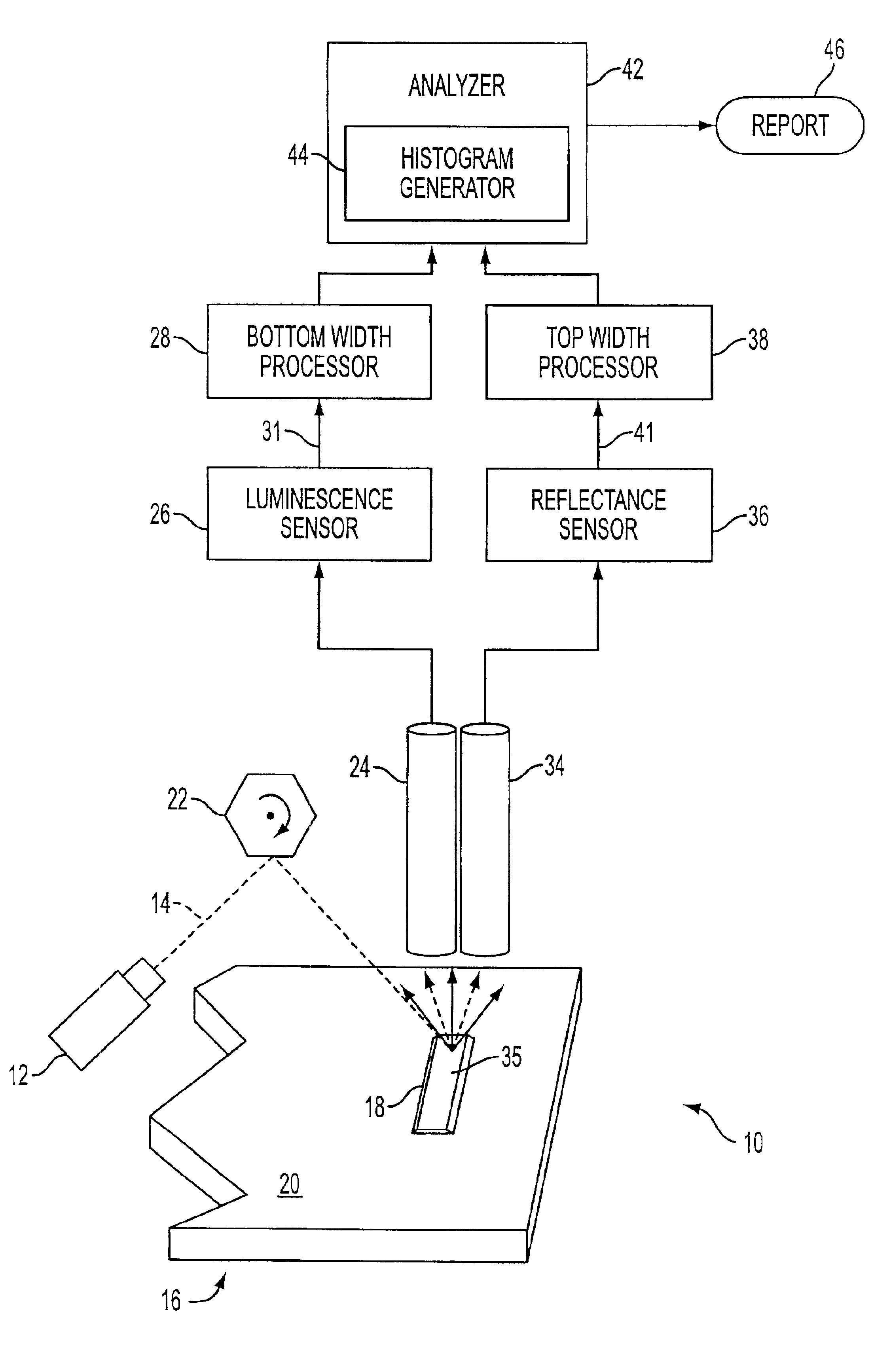
In FIG. 1, automated optical inspection system 10 is operative to inspect electrical circuits for defects in accordance with an embodiment of the present invention.

AOI system 10 suitably is a V-300 automated optical inspection system available from Orbotech Ltd., of Yavne Israel. Such a system is described in U.S. Pat. No. 5,216,479 to Dotan et al., which issued on Jun. 1, 1993, the disclosure of which is incorporated by reference in its entirety for its useful information on optical inspection systems.

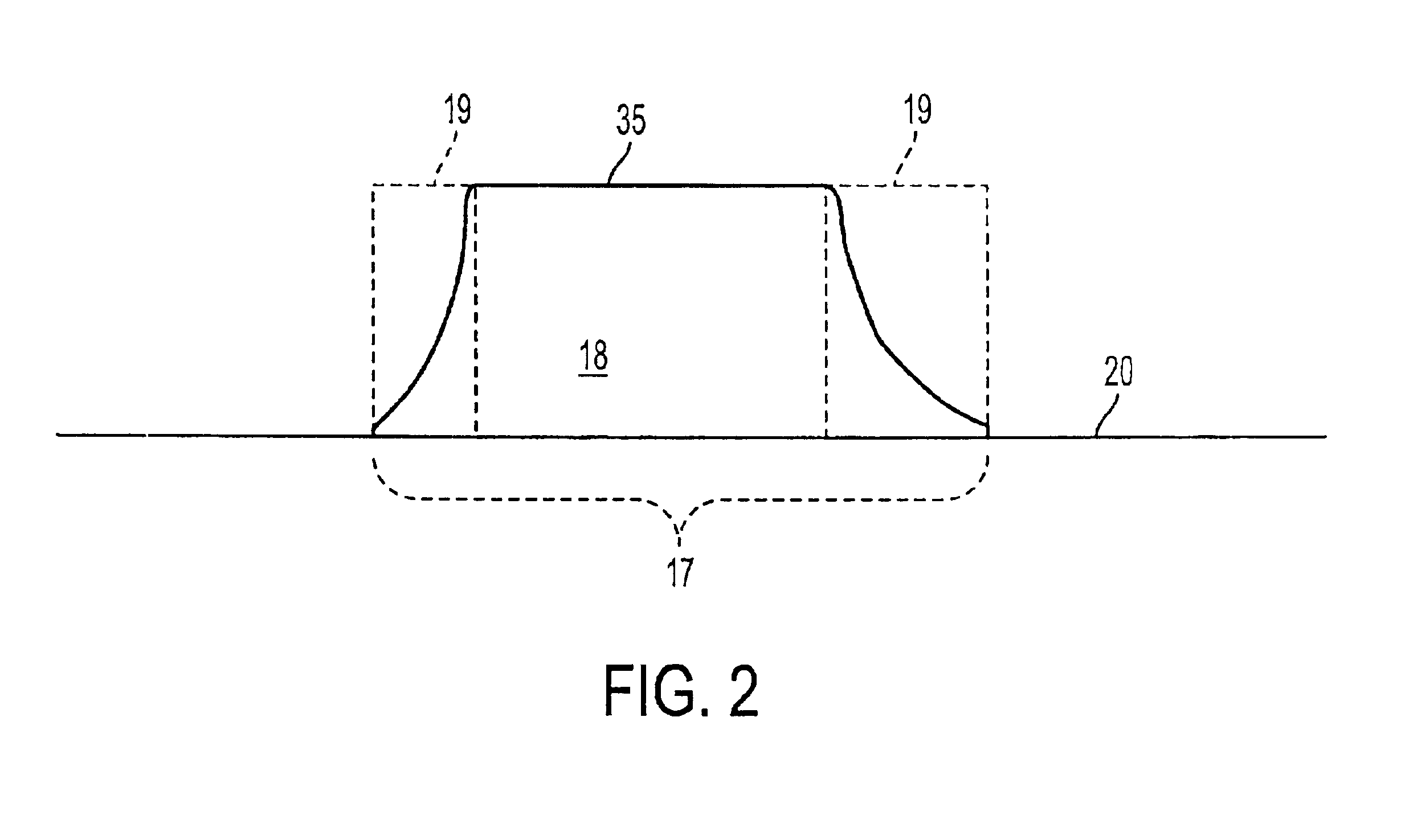
In FIG. 1, reference numeral 12 indicates a source of radiant energy; reference numeral 14 indicates a beam of radiant energ...


PUM


Abstract

A first inspection functionality is provided to obtain information about a first attribute at a conductor location on an electrical circuit. A second inspection functionality is provided to obtain information about a second attribute at the conductor location. A combination of first attribute information and second attribute information is analyzed to determine an inspection attribute of the conductor at the conductor location. Attribute information may relate to one or more of: reflectance, fluorescence or height.

Description

FIELD OF THE INVENTIONThis description generally relates to the field of electrical circuit inspection. More particularly, the field of interest involves systems and methods for fabricating and inspecting electrical circuit conductors in electrical circuits.BACKGROUND OF THE INVENTIONThe production of printed circuit boards is an expensive undertaking, and many extraordinary measures are routinely taken to ensure the highest possible production quality. Automated optical inspection (AOI) harnesses the power, speed, and reliability of computer technology to assist with the task of inspection of printed circuit boards for defects. Existing automated optical inspection (AOI) systems, such as the PC-14 Micro™ and Blaser™ AOI systems, are available from Orbotech of Yavne, Israel.As used herein, the term “printed circuit board” will be understood to refer in general to any electrical circuit on any substrate, including printed circuit boards, multi-chip modules, ball grid array substrates...

Claims


Application Information

Patent Timeline
IPC IPC(8): G01N21/956G01N21/88
CPCG01N21/95684
Inventor SAVAREIGO, NISSIMMARKOV, IGORZEMER, DAN
Owner ORBOTECH LTD
Why Eureka
Try Eureka