
Memory controller with programmable configuration

a memory controller and configuration technology, applied in the field of memory controllers, can solve problems such as affecting the performance of memory systems

Inactive Publication Date: 2005-04-05
AVAGO TECH INT SALES PTE LTD
View PDF17 Cites 293 Cited by
  • Summary
  • Abstract
  • Description
  • Claims
  • Application Information

AI Technical Summary

Benefits of technology

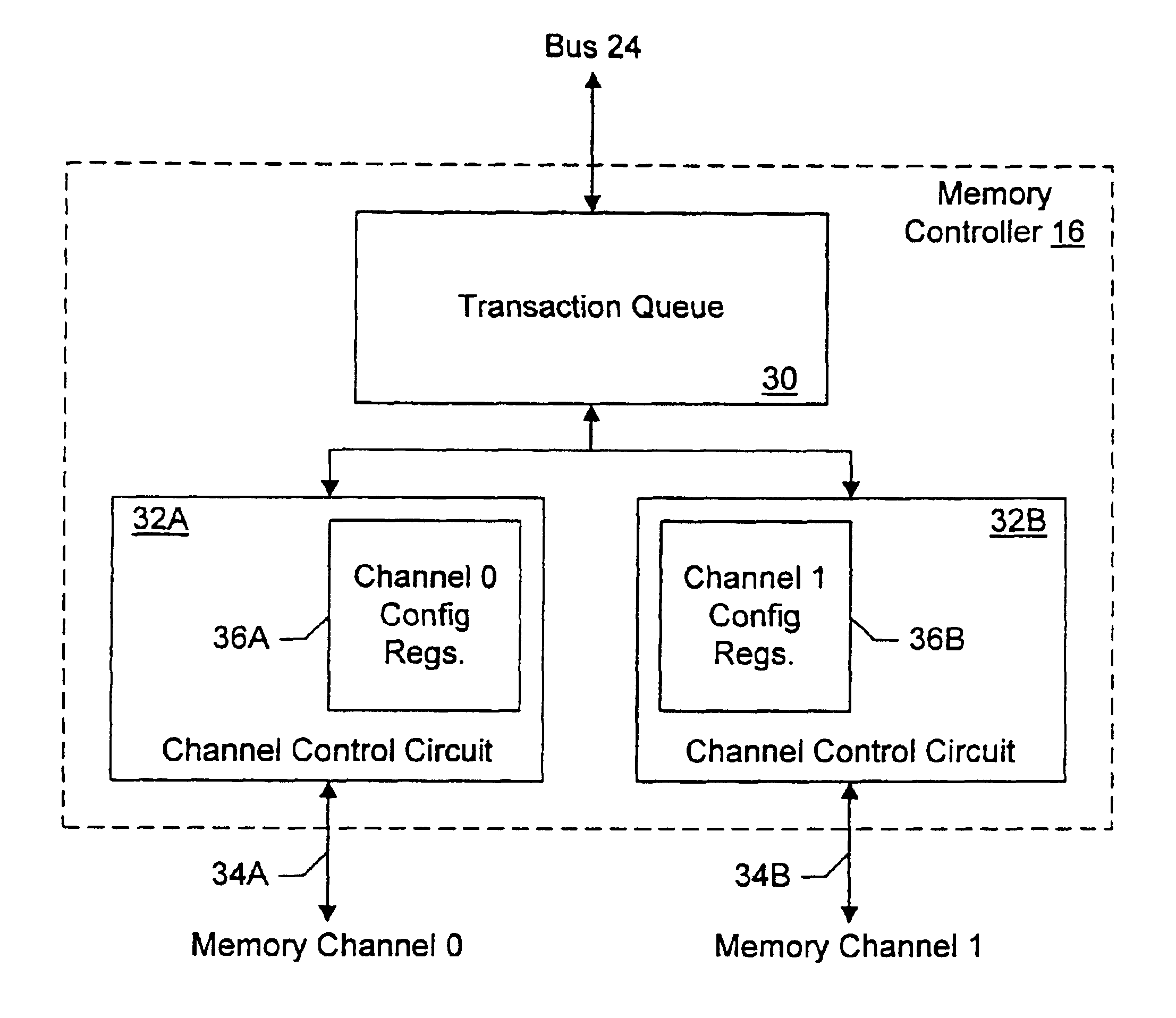
The problems outlined above are in large part solved by a memory controller as described herein. The memory controller provides programmable flexibility, via one or more configuration registers, for the configuration of the memory. The memory may be optimized for a given application by programming the configuration registers. For example, in one embodiment, the portion of the address of a memory transaction used to select a storage location for access in response to the memory transaction may be programmable. In an implementation designed for DRAM, a first portion may be programmably selected to form the row address and a second portion may be programmable selected to form the column address. Additional embodiments may further include programmable selection of the portion of the address used to select a bank. By allowing the row address, column address, and bank selection to be programmably selected from the address, the memory system may be optimized by software for the expected memory access patterns. If memory transactions, clustered relatively close in time, are expected to traverse through large blocks of memory, the bank selection may be drawn from more significant bits than the column selection, for example, allowing the memory transactions to experience an open page timing while leaving other banks available for intervening memory transactions to other addresses.
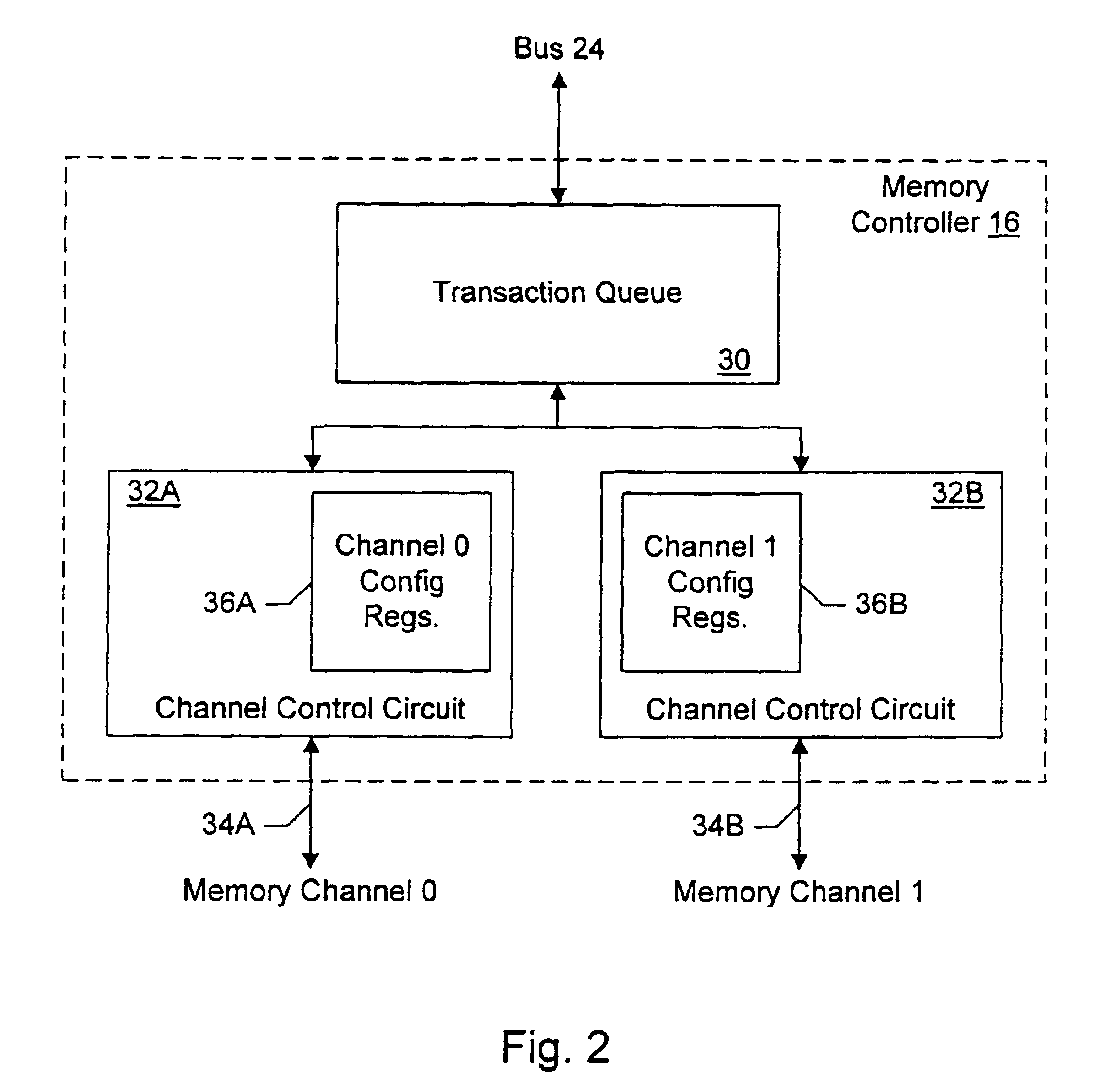
Still further, interleave modes among memory sections assigned to different chip selects and among two or more channels to memory may be programmable, in some implementations. Furthermore, the portion of the address used to select between interleaved memory sections or interleaved channels may be programmable. Having the interleave, or lack thereof, of memory sections or channels programmable may also provide for flexibility. For example, if accesses to certain address ranges are expected to be accessed with multiple memory transactions clustered close in time, then those address ranges may be represented by two or more interleaved memory sections or channels. Since pages may be open in each of the interleaved memory sections, the interleaving may increase the possibility of receiving transactions which access an open page. On the other hand, other address ranges may not be expected to be accessed with multiple clustered memory transactions, and thus the corresponding memory section or channels may be configured as non-interleaved. The non-interleaved memory sections or channels may have more open pages at different addresses, allowing for different transactions to access an open page.
One particular implementation may include all of the above programmable features, which may provide a high degree of flexibility in optimizing the memory system.

Problems solved by technology

Furthermore, depending upon the arrangement of data in memory, the portions of the address of a memory transaction used to select a storage location in the memory corresponding to the address may affect the performance of the memory system.
Unfortunately, memory controllers have generally been implemented with a relatively fixed configuration.

Method used


Image

  • Memory controller with programmable configuration
  • Memory controller with programmable configuration
  • Memory controller with programmable configuration

Examples


examples 120-124

Examples 120-124 illustrate some of the flexibility available in configuring the memory by configuring the selection of row address, column address, and bank selection. In the configuration of the example 120, the bank selection is selected from the least significant bits out of the row address, column address, and bank selection. Thus, if a set of consecutive memory accesses accessed contiguous cache lines (which are 32 bytes in the illustrated embodiment), the bank selection would change each time before the column address changes. Thus, at least a few of the set of consecutive memory transactions might not encounter an open page, but subsequent transactions of the set might encounter open pages in each bank. On the other hand, the configuration of example 122 may provide an open page for up to 1K contiguous cache lines, all in the same bank. The pages open in other banks may not be affected by the set of consecutive memory transactions. Example 124 would provide an open page for ...


PUM


Abstract

A memory controller provides programmable flexibility, via one or more configuration registers, for the configuration of the memory. The memory may be optimized for a given application by programming the configuration registers. For example, in one embodiment, the portion of the address of a memory transaction used to select a storage location for access in response to the memory transaction may be programmable. In an implementation designed for DRAM, a first portion may be programmably selected to form the row address and a second portion may be programmable selected to form the column address. Additional embodiments may further include programmable selection of the portion of the address used to select a bank. Still further, interleave modes among memory sections assigned to different chip selects and among two or more channels to memory may be programmable, in some implementations. Furthermore, the portion of the address used to select between interleaved memory sections or interleaved channels may be programmable. One particular implementation may include all of the above programmable features, which may provide a high degree of flexibility in optimizing the memory system.

Description

BACKGROUND OF THE INVENTION1. Field of the InventionThis invention is related to the field of memory controllers.2. Description of the Related ArtMemory controllers are generally included in systems to interface various devices in the system with the memory. Generally, the memory controller receives a memory transaction, which includes an address, from one of the devices and accesses the memory using the address. More particularly, the memory controller may use a portion of the address to select a storage location in the memory for access in response to the memory transaction. In a typical dynamic random access memory (DRAM) controller, for example, a first portion of the address is a row address for the DRAM and a second portion of the address is a column address for the DRAM. Together, the row and column addresses select a storage location in the DRAM to be accessed in response to the memory transaction.Various memory controllers have implemented other features as well. For exampl...

Claims


Application Information

Patent Timeline
Patent Type & Authority Patents(United States)
IPC IPC(8): G06F12/06G06F12/02
CPCG06F12/0653G06F12/0607G06F12/0215
Inventor CHO, JAMES Y.KELLER, JAMES B.HAYTER, MARK D.
Owner AVAGO TECH INT SALES PTE LTD
Learn More