Glitch removal circuit

a technology of glitch removal and circuit, which is applied in the field of circuits, can solve the problems of short overshoot period, noisy environment of electrical circuits, and noise generation of spurious components in the input or output signals of circuits

Inactive Publication Date: 2005-05-17
NORTH STAR INNOVATIONS
View PDF15 Cites 17 Cited by
  • Summary
  • Abstract
  • Description
  • Claims
  • Application Information

AI Technical Summary

Problems solved by technology

Electrical circuits often have to operate in noisy environments.
Such noise generates spurious components in the input or output signals of the circuit.
A positive glitch may occur on a logic low signal causing it to overshoot for a brief period.
Similarly, a negative glitch may occur on a logic high signal causing it to undershoot for a brief period.
Glitches, if untreated, may affect the operation of a circuit and hamper the performance of the entire system of which the circuit is a part.
In digital systems, glitches may tamper with clock signals and handshake signals that drive various circuits within the system.
For example, in a memory array if a glitch occurs in an address signal while it is being latched, then the wrong address may be read, which may lead to an unrecoverable system error.
Also, glitches may cause chips to receive or transmit noisy signals to other chips.
Existing glitch removal circuits suffer from a number of drawbacks, such as being overly complex, requiring a large number of components, and requiring a large amount of space.
Hence, these circuits are difficult to implement, use valuable chip real estate, and draw excess current.
Further, such circuits may also introduce an excessively long delay in the output signal as compared with the duration of the glitch to be filtered, leading to slow signal processing speeds.
This may also affect the synchronization of output signals with other circuits.

Method used


Image

  • Glitch removal circuit
  • Glitch removal circuit
  • Glitch removal circuit

Examples


Embodiment Construction

[0015]The detailed description set forth below in connection with the appended drawings is intended as a description of the presently preferred embodiments of the invention, and is not intended to represent the only form in which the present invention may be practiced. It is to be understood that the same or equivalent functions may be accomplished by different embodiments that are intended to be encompassed within the spirit and scope of the invention.

[0016]For convenience, terms that have been used in the description of various embodiments are defined below. These definitions are provided merely to aid the understanding of the description, and are not to be construed as limiting the scope of the invention.

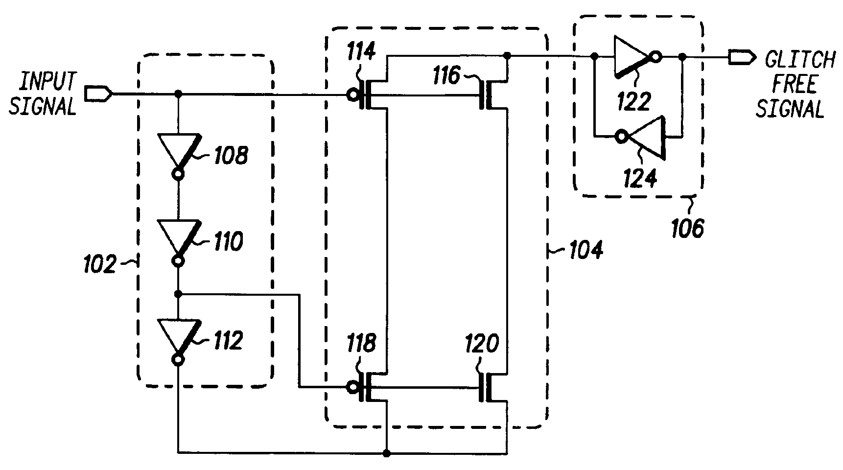
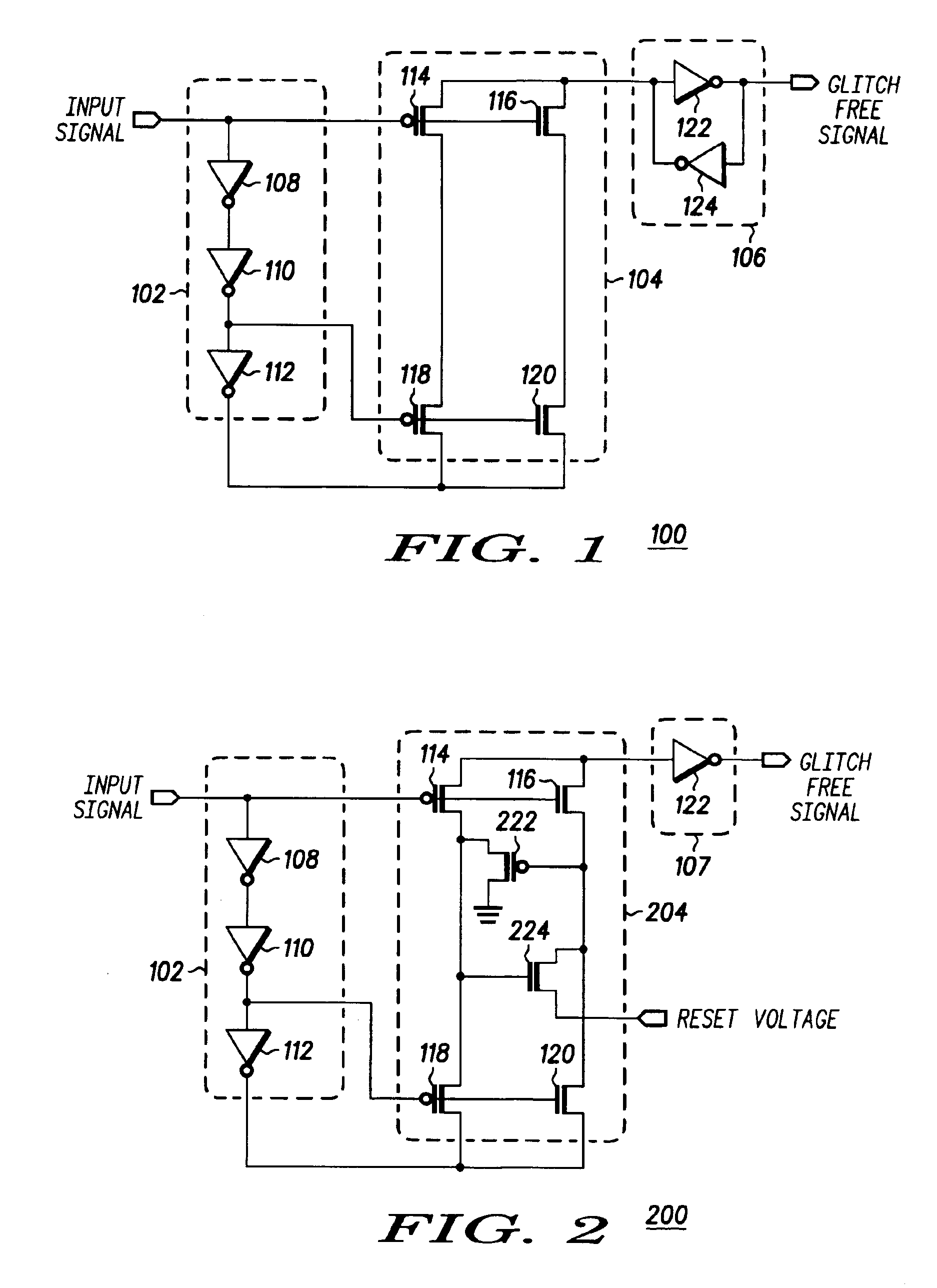
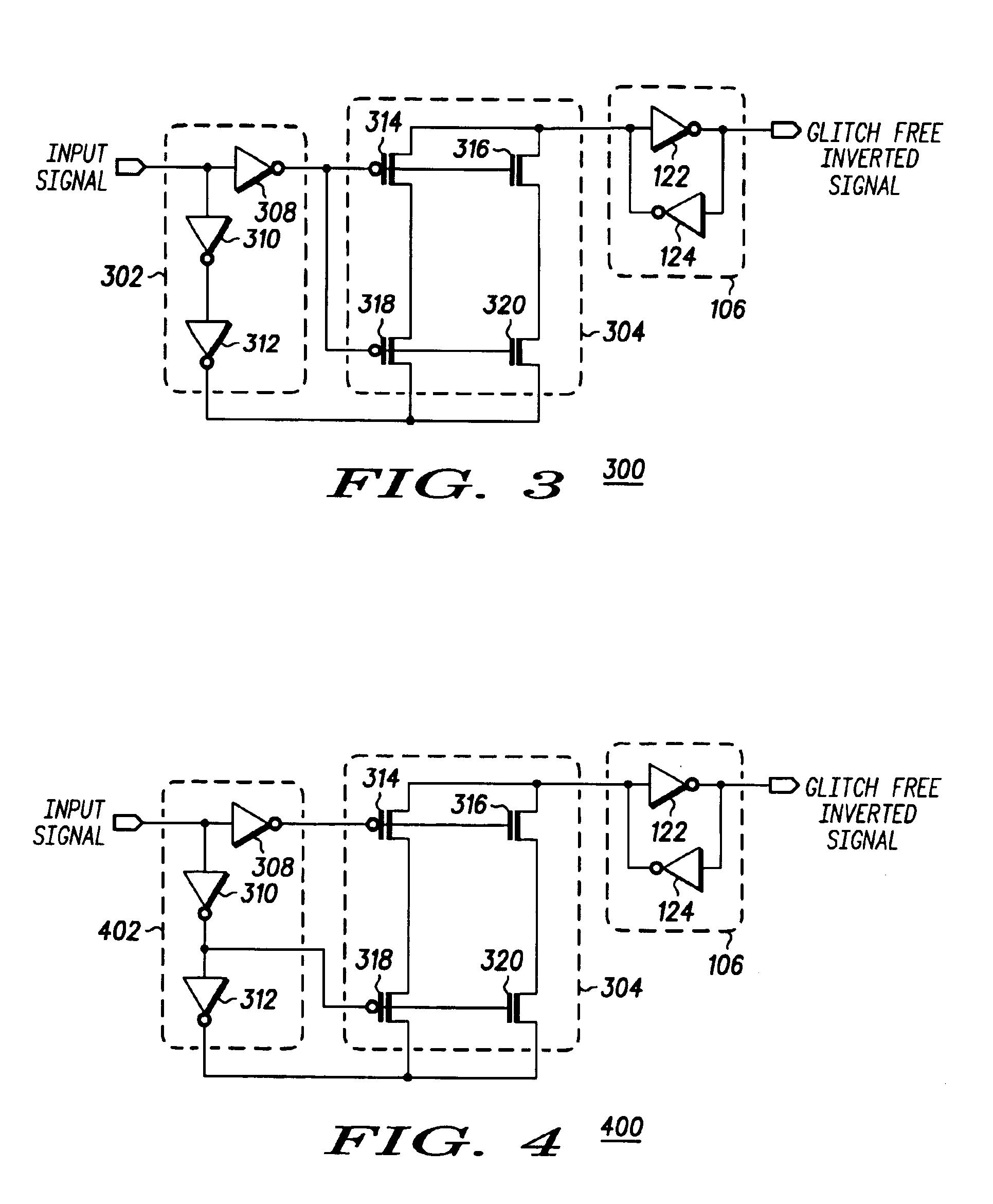
[0017]GRW—GRW is an acronym for Glitch Removal Width, which is the width of the maximum width glitch that can be removed from the input signal by a glitch removal circuit. It is desirable to have a high GRW for a glitch removal circuit.

[0018]PRI—PRI is an acronym for Performance ...


PUM


Abstract

A glitch removal circuit that removes both positive and negative glitches from an input signal includes a delay circuit, a glitch blocking circuit, and a latch circuit. The delay circuit receives the input signal and introduces a delay into it. The glitch blocking circuit is coupled to the delay circuit, and includes two NMOS transistors and two PMOS transistors. The glitch blocking circuit receives the input signal and the delayed input signal and blocks the input signal if there is a glitch in it. The latch circuit is coupled to the output of the glitch blocking circuit. The latch circuit inverts the output of the glitch blocking circuit and stores the output on a continuous basis. The latch circuit provides glitch free signal as the output.

Description

BACKGROUND OF THE INVENTION[0001]The present invention relates to a circuit for removing unwanted glitches from signals and more particularly, to a glitch removal circuit that removes both positive and negative glitches from signals.[0002]Electrical circuits often have to operate in noisy environments. Noise may be introduced into signals from a number of different sources such as cross talk between signal lines, transients caused by logic gates, electromagnetic interactions between various circuits, etc. Such noise generates spurious components in the input or output signals of the circuit. These spurious components are referred to as glitches.[0003]Glitches distort the size and shape of the signal pulse. A glitch may cause a high signal to become low or a low signal to become high. A positive glitch may occur on a logic low signal causing it to overshoot for a brief period. Similarly, a negative glitch may occur on a logic high signal causing it to undershoot for a brief period.[0...

Claims


Application Information

Patent Timeline
Patent Type & Authority Patents(United States)
IPC IPC(8): H03K5/00H03K5/1252
CPCH03K5/1252
Inventor ALI, SHAHIDDHARNE, SHIVRAJ G.
Owner NORTH STAR INNOVATIONS
Why Eureka
Try Eureka