Data writing and reading methods for flash memories and circuitry thereof

Inactive Publication Date: 2005-05-17
LEADTEK
View PDF3 Cites 1 Cited by
  • Summary
  • Abstract
  • Description
  • Claims
  • Application Information

AI Technical Summary

Benefits of technology

[0008]The present invention uses two flash memories integrated with two individual data writing signal lines to decrease the waiting time for data writing, and thus the performance is as the DDR (double data rate) effect of a DRAM. Therefore, the manner of the present invention can approximately double the writing speed compared to that of the prior art.
[0009]The data writing and reading methods for flash memories of the present invention use two flash memories in connection with a data bus in parallel, and two data writing or reading signal lines respectively electrically connected to each flash memory. The data writing or reading timings of flash memories are controlled by two non-overlapping data writing or reading signals, which may differ from each other by 180°, thereby data can be written into or be read from the flash memory so as to increase the data writing or reading efficiency.
[0012]Ideally, the data writing method of the present invention can double the writing speed compared to the traditional manner, and a further 20% speed improvement can be obtained by employing data flow processing. As a result, the access speed and programming speed can respectively ramp up to 50 Mbps and 20 Mbps, the instant speed is approximately equivalent to the upper limit of USB2.0, and the average speed is approximately equivalent to the speed of USB1.1 multiplied 20, so the efficiency of the data writing speed of flash memories can be significantly increased.
[0013]Although the main objective of the present invention is to increase the data writing speed of flash memories, it can also apply to the data reading of flash memories. In comparison with the data writing circuitry, data reading circuitry is in connection with a data bus in parallel as well, except the two data writing signal lines electrically connected to flash memories are replaced with two data reading signal lines. The data reading timing of flash memories is controlled by two non-overlapping or phase-shifted by 180° reading signals.

Problems solved by technology

However, the writing speed cannot keep up with the reading speed, so usually the product cannot perform optimally.
The implementation of such a temporary-save manner needs only one flash memory, but the writing efficiency is not good enough.
Therefore, the data transmission speed usually becomes a speed bottleneck of the USB disk.
Although the above-mentioned methods can improve the data writing efficiency of flash memories, which are still limited to the applications of the electronic devices demanding more high data transmission speed, there is still large room for improvement.

Method used


Image

  • Data writing and reading methods for flash memories and circuitry thereof
  • Data writing and reading methods for flash memories and circuitry thereof
  • Data writing and reading methods for flash memories and circuitry thereof

Examples


Embodiment Construction

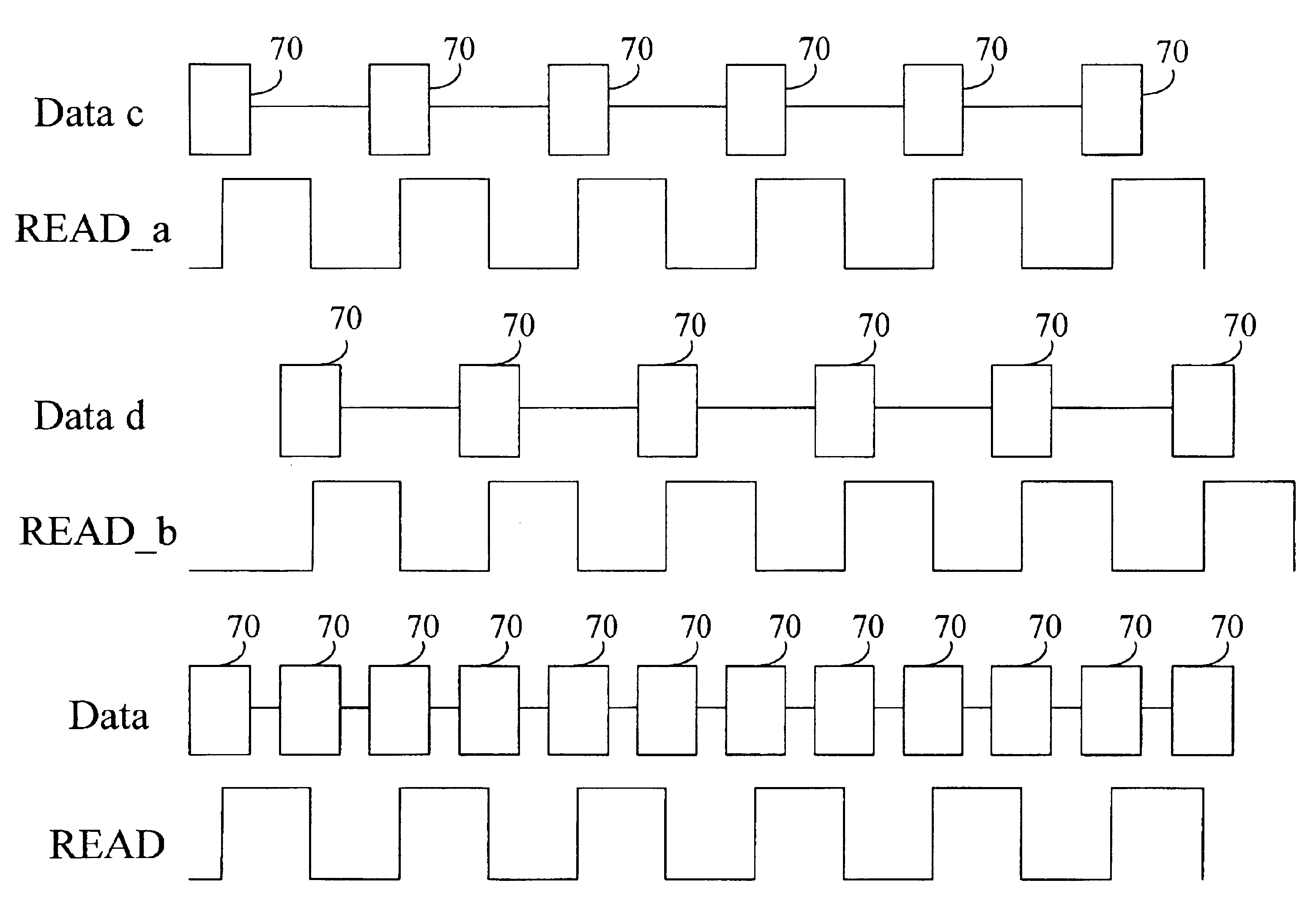
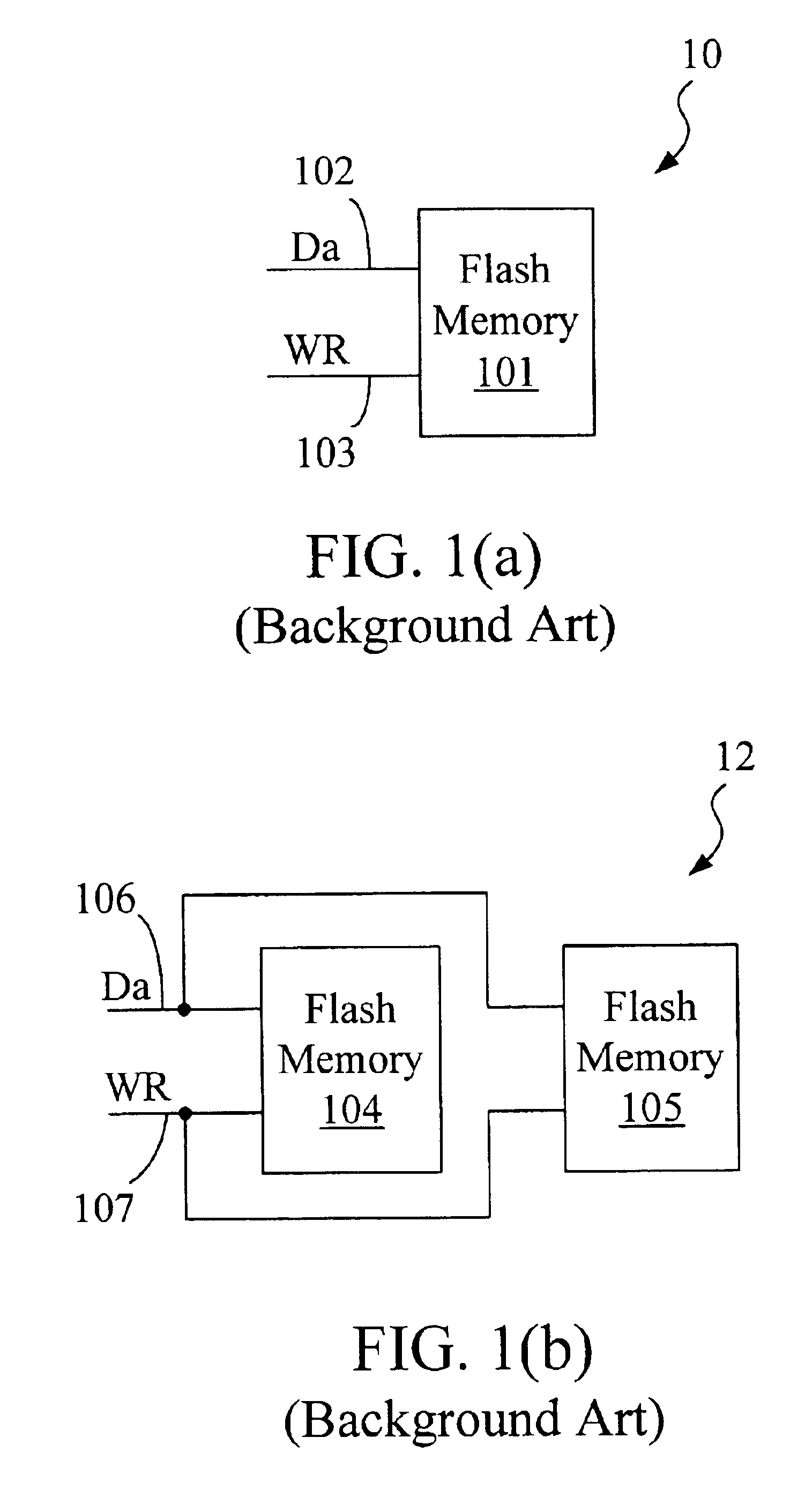
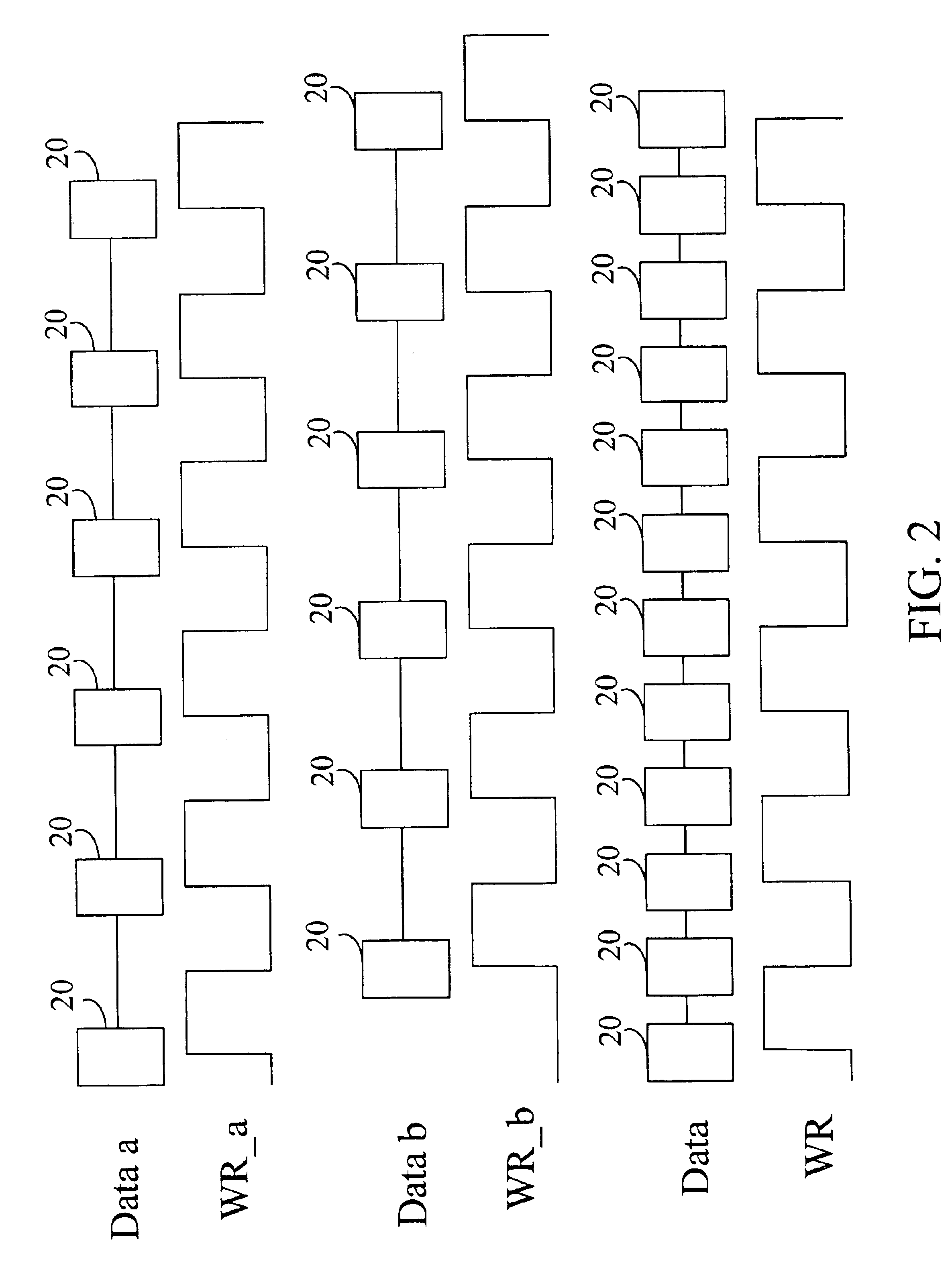
[0022]Referring to FIG. 2, the data writing for flash memories by a known temporary-save or a circulation manner is shown as Data_a. When a data writing signal WR_a switches from a low level to a high level, data 20 is going to be written into the flash memories. Accordingly, data 20 is delayed in being written into the flash memory after the previous data 20 by an interval. The present invention is like adding another Data_b to the Data_a, and the data writing timings are controlled by data writing signals WR_a and WR_b. In accordance with the present invention, the data bus is connected to flash memories in parallel, and the data writing signal lines for transmitting WR_a and WR_b are separate. Integrally, the Data_a is accessed or read at the rising edge of a signal WR, and the Data_b is accessed or read at the descending edge of that. As a result, the intervals between the data 20 can be significantly decreased, and approximately double the data can be written during the same ti...


PUM


Abstract

Data writing and reading methods and the implementation circuitry is revealed, in which two flash memories are connected to a data bus in parallel, and two data writing or reading signal lines are respectively electrically connected to each flash memory. The data writing or reading timings of flash memories are controlled by two non-overlapping data writing or reading signals, which may differ from each other by 180°, thereby data can be written into or read from the flash memory so as to increase the data writing and reading efficiencies.

Description

BACKGROUND OF THE INVENTION[0001](A) Field of the Invention[0002]The present invention is related to data writing and reading methods for flash memories and circuitry thereof, more specifically, to methods and their implementation circuitry so that data can be written to or read from flash memories in the same time period.[0003](B) Description of Related Art[0004]These days, the reading speed of a related flash memory product is becoming more rapid. However, the writing speed cannot keep up with the reading speed, so usually the product cannot perform optimally. Because the manner of writing and the related implementation for writing speed enhancement are not standardized yet, employing current standard flash memories is the most feasible way to increase the writing speed.[0005]The methods for enhancing the writing speed of a flash memory or flash memories can be attained by the following methods. First, employing a temporary-save manner, by which data is temporarily saved in a buff...

Claims


Application Information

Patent Timeline
IPC IPC(8): G11C16/10G11C16/26G11C16/06G11C7/10
CPCG11C7/1042G11C16/26G11C16/10
Inventor CHUANG, MIKE
Owner LEADTEK
Why Eureka
Try Eureka