Power module

a power module and power module technology, applied in the direction of basic electric elements, electrical apparatus contruction details, printed circuit non-printed electric components association, etc., can solve the problems of increasing circuit inductance, large number of parts, complicated assembly, etc., to reduce circuit inductance, shorten the wiring path, and enhance the reliability of the power module

Inactive Publication Date: 2005-05-31
MITSUBISHI ELECTRIC CORP +1
View PDF18 Cites 25 Cited by
  • Summary
  • Abstract
  • Description
  • Claims
  • Application Information

AI Technical Summary

Benefits of technology

[0041]The power module according to the twelfth aspect of the present invention can significantly shorten the wiring path between the smoothing capacitor and the power semiconductor device to greatly reduce the circuit inductance.
[0042]The power module according to the thirteenth aspect of the present invention can make the smoothing capacitor and the insulating substrate equal in thermal expansion coefficient, to avoid various disadvantages resulting from the difference in thermal expansion coefficient, thereby enhancing the reliability of the power module.
[0043]The power module according to the fourteenth aspect of the present invention can effectively dissipate the heat generated by the smoothing capacitor through the heat sink to the outside.
[0044]In the power module according to the fifteenth aspect of the present invention, the cooling fin can effectively cool down the smoothing capacitor to enhance the reliability of the power module.
[0045]In the power module according to the sixteenth aspect of the present invention, the use of the ceramic capacitor having good charging and discharging properties increases the operating speed of the power module.
[0046]It is therefore an object of the present invention to provide a power module which can reduce a circuit inductance and which is small in size, light in weight and high in resistance to vibration.

Problems solved by technology

This presents problems in the large number of parts and in complicated assembly.
Another problem is an increased circuit inductance because of a long wiring path between the smoothing capacitors 120 and the power semiconductor devices 105.

Method used


Image

  • Power module
  • Power module
  • Power module

Examples


first preferred embodiment

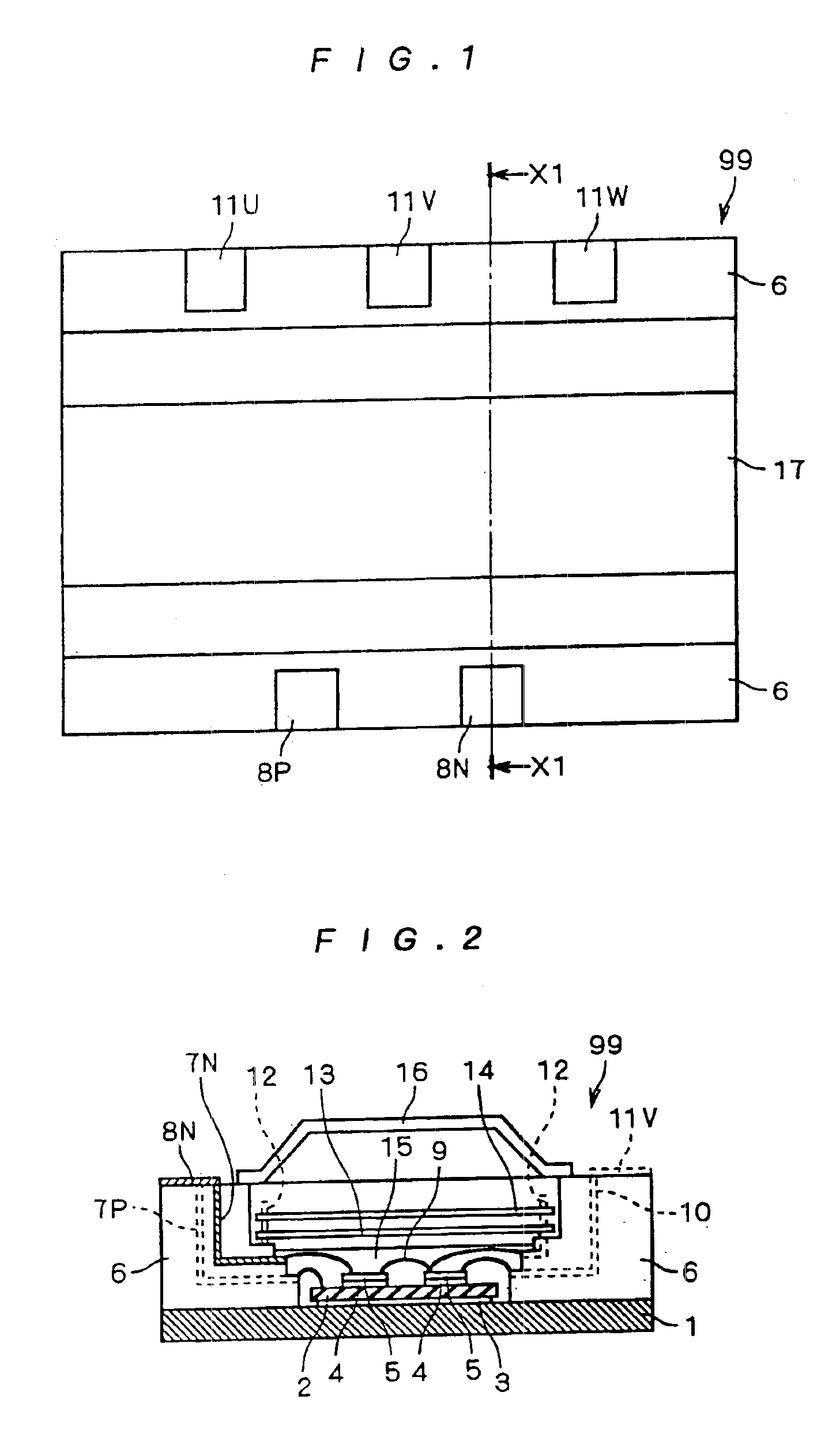
[0078]FIG. 1 is a top plan view schematically showing a structure of a power module body portion 99 according to a first preferred embodiment of the present invention. Output terminals 11U, 11V and 11W corresponding to three U-, V- and W-phases respectively are arranged along a first side of a top surface of a case frame 6. An N-terminal 8N and a P-terminal 8P are arranged along a second side of the top surface of the case frame 6 which is parallel to the first side.

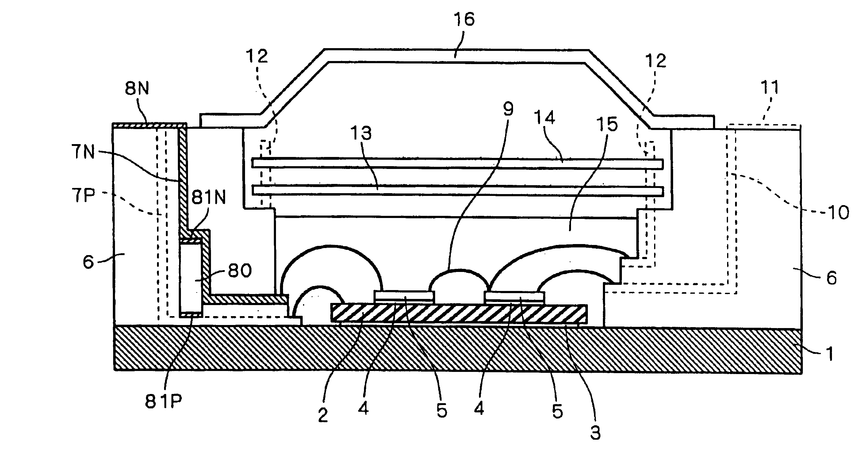
[0079]FIG. 2 is a cross-sectional view showing a cross-sectional structure taken along the line X1—X1 of FIG. 1. The case frame 6 made of resin is disposed on a metal base plate 1 functioning as a heat sink, and a case lid 16 made of resin is disposed on the case frame 6. An insulating substrate 2 made of ceramic is soldered, as shown at 3, onto the base plate 1. A plurality of power semiconductor devices 5 such as IGBTs are mounted on the insulating substrate 2 with solder 4. Circuit elements (not shown) such as switchi...

second preferred embodiment

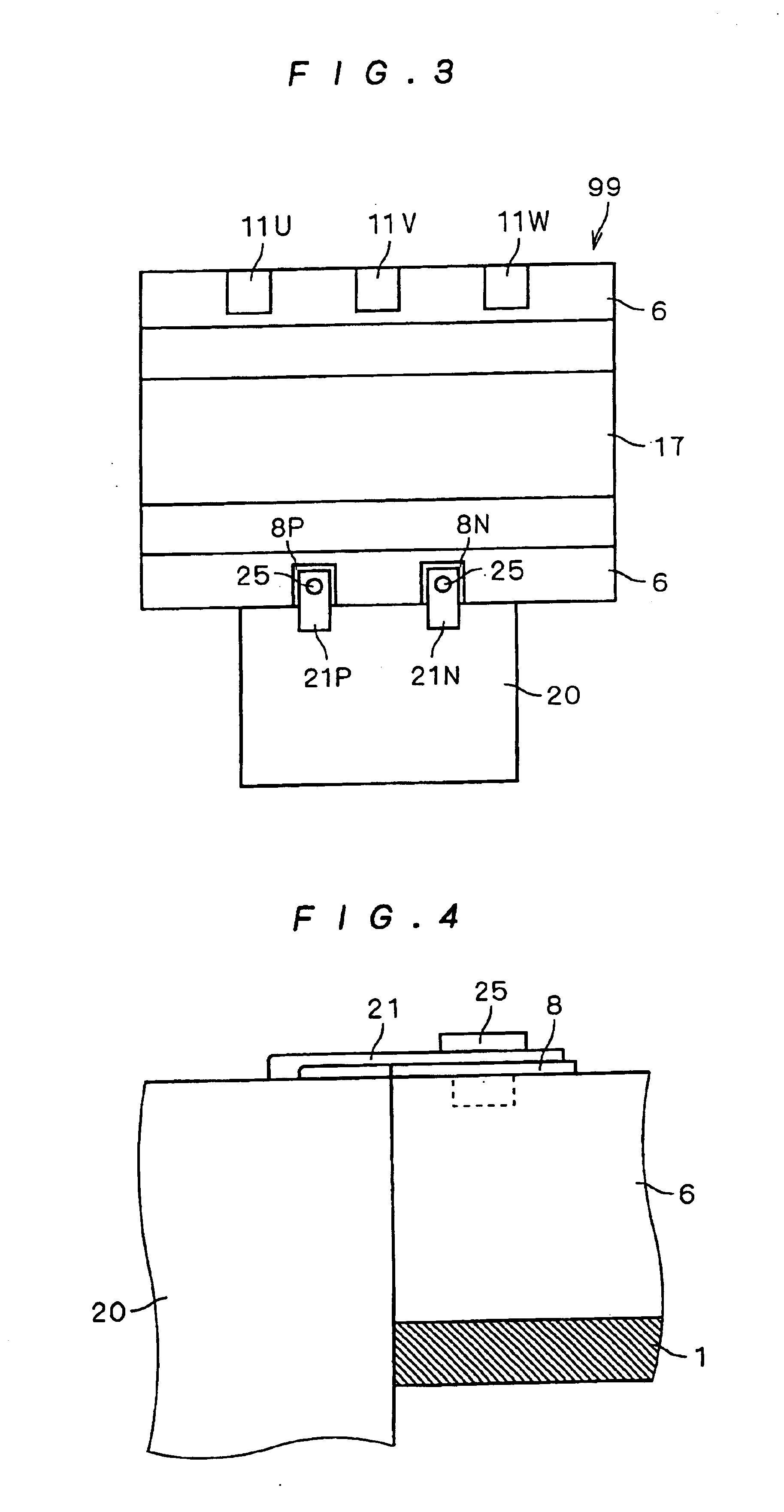
[0091]FIG. 7 is a top plan view schematically showing the overall construction of the power module according to a second preferred embodiment of the present invention. FIGS. 8 and 9 are cross-sectional views showing cross-sectional structures taken along the lines X2—X2 and X3—X3 of FIG. 7, respectively. With reference to FIG. 7, a plurality of capacitor elements 30a to 30e are arranged in a smoothing capacitor enclosure 32. Referring to FIG. 8, the capacitor elements 30a to 30e have N-electrodes 35a to 35e at their bottom surfaces, respectively. The N-electrodes 35a to 35e are commonly in contact with the plate-shaped N-electrode 21N. Part of the N-electrode 21N extends to a top surface of the enclosure 32 and is fastened by the screw 25 to the N-terminal 8N of the power module body portion 99.

[0092]Referring to FIG. 9, the capacitor elements 30a to 30e have P-electrodes 36a to 36e at their top surfaces, respectively. The P-electrodes 36a to 36e are commonly in contact with the pla...

third preferred embodiment

[0098]FIG. 11 is a top plan view schematically showing the overall construction of the power module according to a third preferred embodiment of the present invention. FIG. 12 is a cross-sectional view showing a cross-sectional structure taken along the line X4—X4 of FIG. 11. An outer surface of the case frame 6 includes a partial recess having a pair of opposed side surfaces. The N-terminal 8N is disposed on a first one of the side surfaces of the recess, and the P-terminal 8P is disposed on a second one thereof. As shown in FIG. 12, the N-terminal 8N and the P-terminal 8P extend to parts of the top surface of the case frame 6 which surround the recess.

[0099]A smoothing capacitor 40 is shaped to fit in the recess, and has an N-electrode 43N on its first side surface opposed to the first side surface of the recess and a P-electrode 43P on its second side surface opposed to the second side surface of the recess. The smoothing capacitor 40 is fitted in the recess, and solder 41 bonds ...


PUM


Abstract

A power module includes a first substrate with a power semiconductor device mounted thereon, a second substrate with a control circuit for controlling the power semiconductor device formed thereon, a smoothing capacitor electrically connected to the power semiconductor device for smoothing a voltage to be externally supplied to the power semiconductor device, and a case including a case frame and a case lid. The case has an interior in which the first substrate, the second substrate and the smoothing capacitor are disposed, and the smoothing capacitor is disposed in contact with a side surface of the case frame.

Description

CROSS-REFERENCE TO RELATED APPLICATIONS[0001]This application is a divisional of U.S. patent application Ser. No. 10 / 314,989, filed Dec. 10, 2002 now U.S. Pat. No. 6,762,937, which is a divisional of U.S. patent application Ser. No. 09 / 690,012, filed Oct. 17, 2000, now U.S. Pat. No. 6,522,544, and claims priority to Japanese patent Application No. 2000-143482, filed May 16, 2000. The entire contents of U.S. patent applications Ser. No. 10 / 314,989 and Ser. No. 09 / 690,012 are incorporated herein by reference.BACKGROUND OF THE INVENTION[0002]1. Field of the Invention[0003]The present invention relates to a power module structure and, more particularly, to a power module structure including a smoothing capacitor for smoothing a DC supply voltage to be externally applied to a power semiconductor device such as an IGBT.[0004]2. Description of the Background Art[0005]FIG. 28 is a schematic top plan view of a structure of a background art power module body portion 100. Output terminals 111U...

Claims


Application Information

Patent Timeline
Patent Type & Authority Patents(United States)
IPC IPC(8): H01L23/50H01L23/02H01L23/58H01L23/057H01L23/60H01L23/48H01L25/07H02M7/00H01L25/18H02M1/00H02M7/04
CPCH02M7/003H01L23/057H01L23/50H01L23/60H01L24/49H01L25/072H01L2924/16152H01L2924/19041H01L2924/1305H01L2224/32225H01L2924/014H01L2924/01033H01L2924/01023H01L24/48H01L2924/1532H01L2924/13055H01L2924/01074H01L2924/01015H01L2924/01014H01L2924/01013H01L2924/01007H01L2924/01004H01L2224/73265H01L2224/49109H01L2224/48227H01L2224/48137H01L2924/19107H01L2924/30105H01L2924/30107H01L2924/3025H01L24/45H01L2224/45124H01L2224/48091H01L2924/00014H01L2924/00H01L2924/351H01L2224/4811
Inventor KIMOTO, NOBUYOSHIYOSHIDA, TAKANOBUYOSHIMATSU, NAOKIKOGA, MASUONAKAJIMA, DAIMAJUMDAR, GOURABFUKADA, MASAKAZU
Owner MITSUBISHI ELECTRIC CORP
Why Eureka
Try Eureka