CMOS TDI image sensor

a technology of image sensor and time delay, applied in the field of time delay and integration image sensor, can solve the problems of inability to achieve charge transfer in the same way, small and inability to achieve the maximum integration time available for each pixel

Inactive Publication Date: 2005-06-14
TELEDYNE DIGITAL IMAGING INC
View PDF10 Cites 78 Cited by
  • Summary
  • Abstract
  • Description
  • Claims
  • Application Information

AI Technical Summary

Problems solved by technology

However, where the relative velocity is large, the maximum integration time available for each pixel is very small.
If the velocity is sufficiently large relative to the illumination level then the image signal may too small to be useful.
Charge transfer cannot be achieved in the same way with CMOS processes, and hence a CMOS approach to TDI has been disfavored.

Method used


Image

  • CMOS TDI image sensor
  • CMOS TDI image sensor
  • CMOS TDI image sensor

Examples


Embodiment Construction

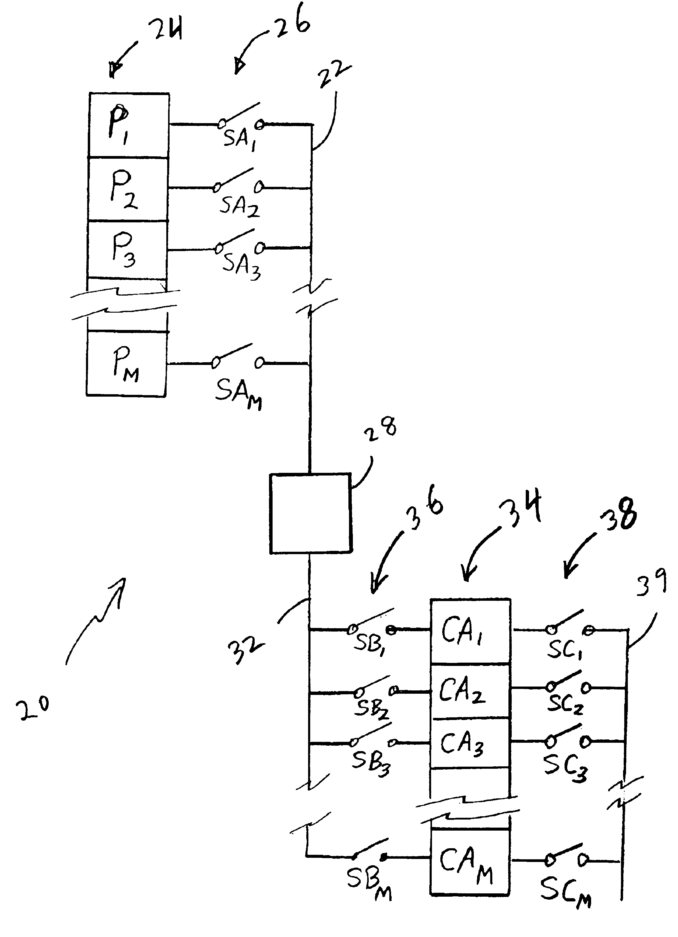
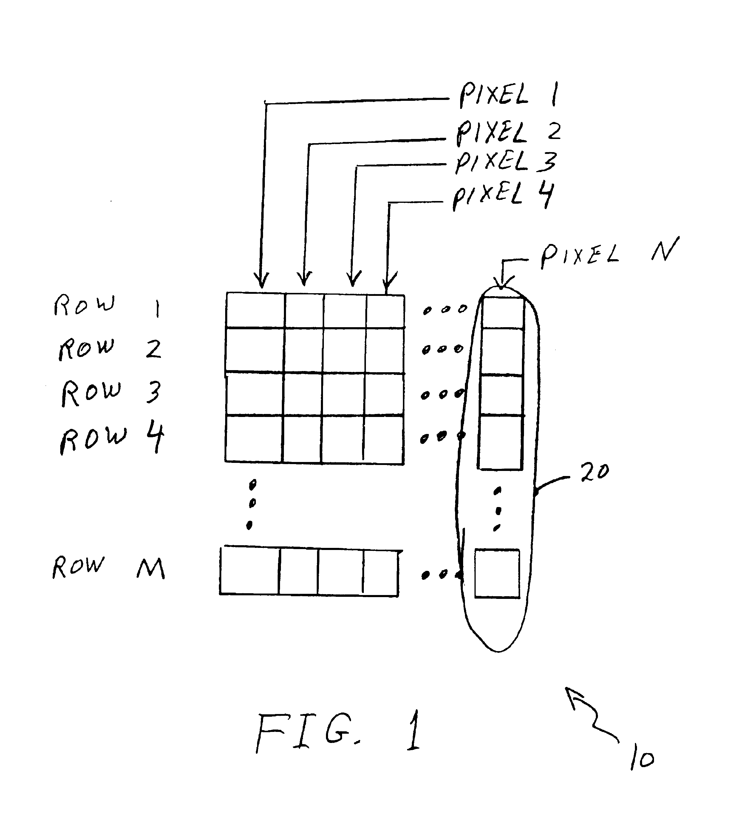
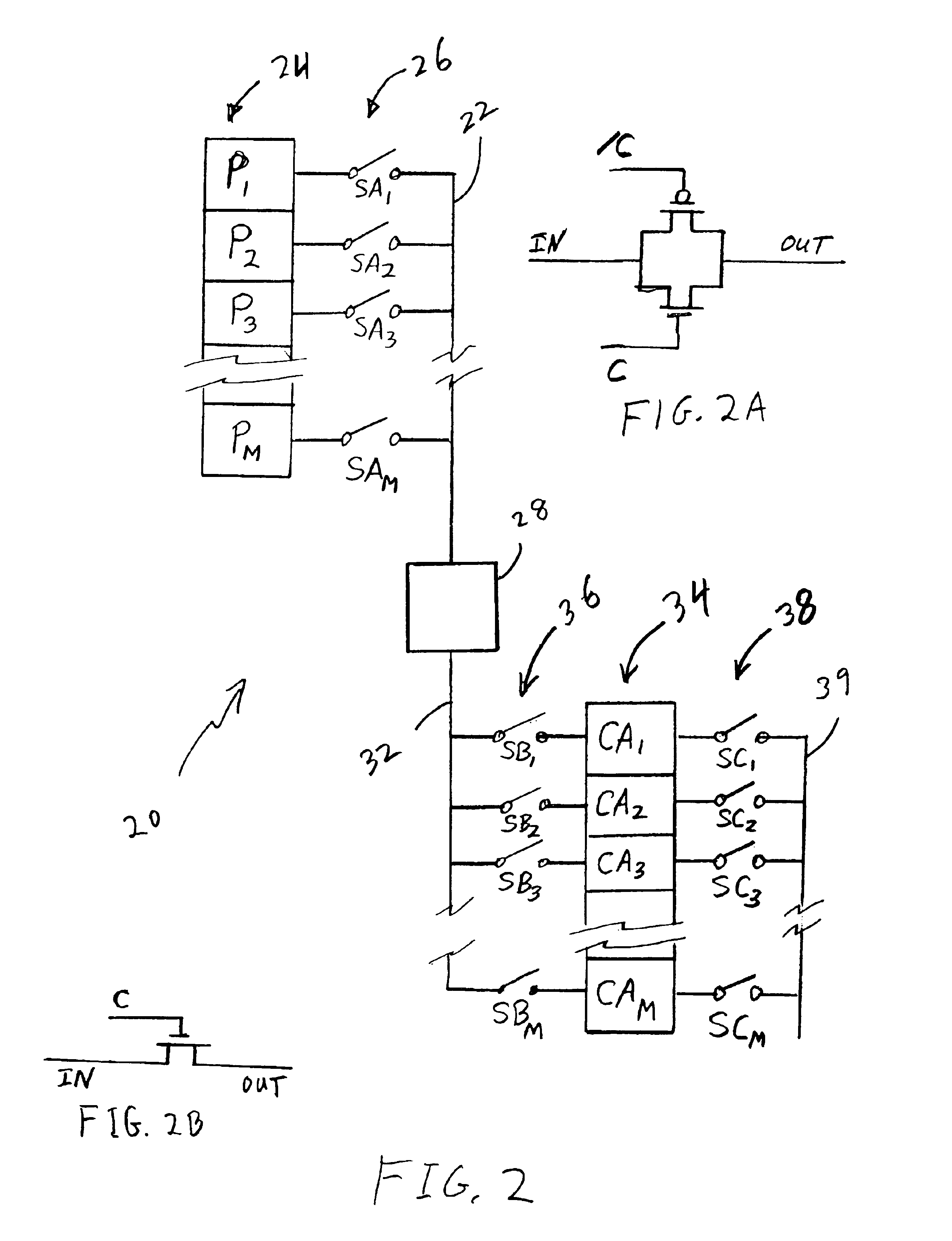
[0019]There are compelling reasons for implementing image sensors with CMOS processes including process accessibility, cost, advanced design rules, and the ability to add circuit functionality that cannot at present be implemented with CMOS processes (digital signal processing, memory, etc.). For example, in instances where a designer of an image sensor does not have an “in house” foundry to fabricate the sensor in wafer form, it becomes necessary to for the designer to contract with a foundry to provide fabrication services. When doing so, the designer usually selects processes and design rules that are supported by a preselected foundry on existing production lines in order to minimize costs. Since CCD processes usually require multiple poly-crystalline silicon conductor layers and CMOS processes require only one such conductor layer, the designer will have greater flexibility using a CMOS process and design rules. The present invention is a way to use a CMOS process and still be ...


PUM


Abstract

A column slice of a CMOS TDI sensor includes a column bus, a column of pixels, plural first switches, a column of accumulators, plural second switches, plural third switches and output bus 39. Each of the plural first switches is coupled between the column bus and a corresponding pixel of the column of pixels, and each of the plural second switches is coupled between the column bus and a corresponding accumulator of the column of accumulators. In operation, only one switch at a time of plural first switches is “on” to connect the voltage signal from a corresponding pixel to the column bus while all remaining plural first switches are “off” to isolate the column bus from all remaining pixels. Only one of the plural second switches is “on” to connect the signal on the column bus to an accumulator while all remaining plural second switches are “off” to isolate the bus from all remaining accumulators. A main control circuit includes first and second shift registers to control the plural first and second switches to couple a signal from each pixel of the column of pixels into a corresponding accumulator of the column of accumulators while updating the accumulator until signals from all pixels have been transferred into corresponding accumulators. After this update cycle, an accumulated signal from the one accumulator that is currently addressed by a third shift register is read to the output. Then, the first and third shift registers are incremented. A new update cycle begins when a point in a moving image focused on the column slice crosses a pixel boundary. The same pattern repeats continuously. Valid TDI data is produced at the output after a number of full cycles of the transfer of pixels signals to the accumulators has been complete, the number being equal to the number of pixels.

Description

[0001]The priority benefit of the Sep. 16, 1998 filing date of U.S. application Ser. No. 60 / 100,558 is hereby claimed.BACKGROUND OF THE INVENTION[0002]1. Field of the Invention[0003]The present invention relates to time delay and integration image sensor (TDI image sensor) using complimentary MOS technology (CMOS technology). In particular, the invention relates to achieving the integration function without charge transfer devices.[0004]2. Description of Related Art[0005]In many imaging applications the image scene moves relative to the camera at a constant velocity. For example, objects on a conveyer belt may be imaged by a stationary camera adjacent to the conveyer, or features on the ground may be imaged by a camera mounted on a moving vehicle. Such applications can be addressed by a line scan camera in which the imaging region consists of a single row of pixels. However, where the relative velocity is large, the maximum integration time available for each pixel is very small. If...

Claims


Application Information

Patent Timeline
Patent Type & Authority Patents(United States)
IPC IPC(8): H04N5/335H04N5/353H04N5/374
CPCH04N3/155H04N5/3743H04N5/335H04N25/768H04N25/00
Inventor FOX, ERIC
Owner TELEDYNE DIGITAL IMAGING INC
Why Eureka
Try Eureka