Current-controlled CMOS circuit using higher voltage supply in low voltage CMOS process

a technology of cmos circuit and current supply, which is applied in the field of integrated circuits, can solve the problems of low switching speed of conventional cmos logic, near zero static power consumption of cmos logic, and limited speed of cmos logic family, so as to achieve high switching speed, dissipate static current, and maximize the effect of speed of operation

US6911855B2Inactive Publication Date: 2005-06-28AVAGO TECH INT SALES PTE LTD
167 Cites 43 Cited by

Patent Information

Authority / Receiving Office
US · United States
Patent Type
Patents(United States)
Current Assignee / Owner
Publication Date
2005-06-28
Estimated Expiration
Not applicable · inactive patent

Smart Images

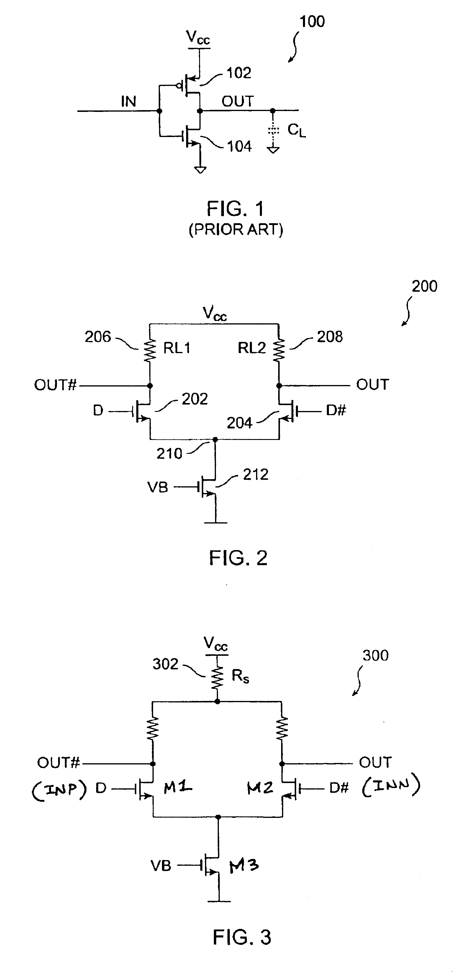
  • Figure 1
    Figure 1
  • Figure 2
    Figure 2
  • Figure 3
    Figure 3
Patent Text Reader

Abstract

Various circuit techniques for implementing ultra high speed circuits use current-controlled CMOS (C3MOS) logic fabricated in conventional CMOS process technology. An entire family of logic elements including inverter / buffers, level shifters, NAND, NOR, XOR gates, latches, flip-flops and the like are implemented using C3MOS techniques. Optimum balance between power consumption and speed for each circuit application is achieve by combining high speed C3MOS logic with low power conventional CMOS logic. The combined C3MOS / CMOS logic allows greater integration of circuits such as high speed transceivers used in fiber optic communication systems. The C3MOS structure enables the use of a power supply voltage that may be larger than the voltage required by the CMOS fabrication process, further enhancing the performance of the circuit.
Need to check novelty before this filing date? Find Prior Art

Description

CROSS-REFERENCES TO RELATED APPLICATIONS

[0001] This application is a Continuation-in-Part of U.S. patent application Ser. No. 09 / 484,856, filed Jan. 18, 2000, now U.S. Pat. No. 6,424,194 B1, which claims priority from U.S. Provisional Patent Application No. 60 / 141,355, filed Jun. 28, 1999, the disclosures of which are each incorporated herein by reference for all purposes.BACKGROUND OF THE INVENTION

[0002] The present invention relates in general to integrated circuitry, and in particular to complementary metal-oxide-semiconductor (CMOS) logic and circuits with enhanced speed characteristics.

[0003] For a number of reasons CMOS is the logic family of choice in today's VLSI devices. Due to the complementary nature of its operation, CMOS logic consumes near zero static power. CMOS also readily scales with technology. These two features are highly desirable given the drastic growth in demand for low power and portable electronic devices. Further, with the computer aided design (CAD) industr...

Examples

Embodiment Construction

[0025]The present invention provides ultra high-speed logic circuitry implemented in silicon complementary metal-oxide-semiconductor (CMOS) process technology. A distinction is made herein between the terminology “CMOS process technology” and “CMOS logic.” CMOS process technology as used herein refers generally to a variety of well established CMOS fabrication processes that form a field-effect transistor over a silicon substrate with a gate terminal typically made of polysilicon material disposed on top of an insulating material such as silicon dioxide. CMOS logic, on the other hand, refers to the use of complementary CMOS transistors (n-channel and p-channel) to form various logic gates and more complex logic circuitry, wherein zero static current is dissipated. The present invention uses current-controlled mechanisms to develop a family of very fast current-controlled CMOS (or C3MOS™) logic that can be fabricated using a variety of conventional CMOS process technologies, but that...