Current-controlled CMOS logic family

a current-controlled, cmos logic technology, applied in the field of integrated circuits, can solve the problems of limited speed of cmos logic family, inability to achieve the highest attainable switching speed, relationship no longer holds in sub-micron technology, etc., to achieve the effect of increasing the speed of operation, discharging static current, and much higher speeds

Inactive Publication Date: 2005-05-31
AVAGO TECH INT SALES PTE LTD
View PDF163 Cites 19 Cited by
  • Summary
  • Abstract
  • Description
  • Claims
  • Application Information

AI Technical Summary

Benefits of technology

[0007]The present invention provides a new family of CMOS logic that is based on current-controlled mechanism to maximize speed of operation. The current-controlled CMOS (or C3MOS™) logic family according to the present invention includes all the building blocks of any other logic family. The basic building block of the C3MOS logic family uses a pair of conventional MOSFETs that steer current between a pair of load devices in response to a difference between a pair of input signals. Thus, unlike conventional CMOS logic, C3MOS logic according to this invention dissipates static current, but operates at much higher speeds. In one embodiment, the present invention combines C3MOS logic with CMOS logic within the same integrated circuitry, where C3MOS is utilized in high speed sections and CMOS is used in the lower speed parts of the circuit.

Problems solved by technology

The one drawback of the CMOS logic family, however, remains its limited speed.
That is, conventional CMOS logic has not achieved the highest attainable switching speeds made possible by modern sub-micron CMOS technologies.
However, this relationship no longer holds in sub-micron technologies.
These alternative technologies, however, have drawbacks of their own that have made them more of a specialized field with limited applications as compared to silicon MOSFET that has had widespread use and support by the industry.
In particular, compound semiconductors such as GaAs are more susceptible to defects that degrade device performance, and suffer from increased gate leakage current and reduced noise margins.
Furthermore, attempts to reliably fabricate a high quality oxide layer using GaAs have not thus far met with success.
This has made it difficult to fabricate GaAs FETs, limiting the GaAs technology to junction field-effect transistors (JFETs) or Schottky barrier metal semiconductor field-effect transistors (MESFETs).
A major drawback of the bipolar technology, among others, is its higher current dissipation even for circuits that operate at lower frequencies.

Method used


Image

  • Current-controlled CMOS logic family
  • Current-controlled CMOS logic family
  • Current-controlled CMOS logic family

Examples


Embodiment Construction

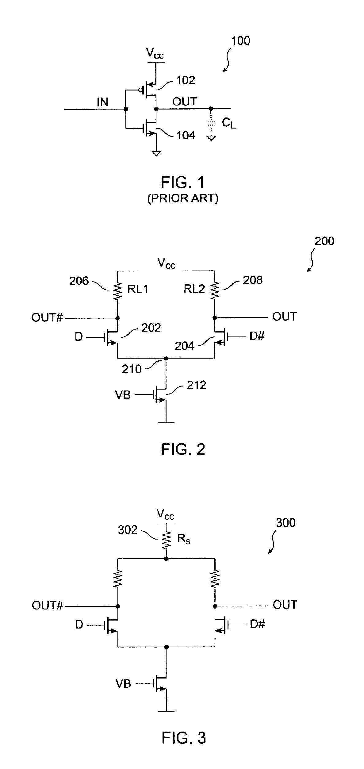
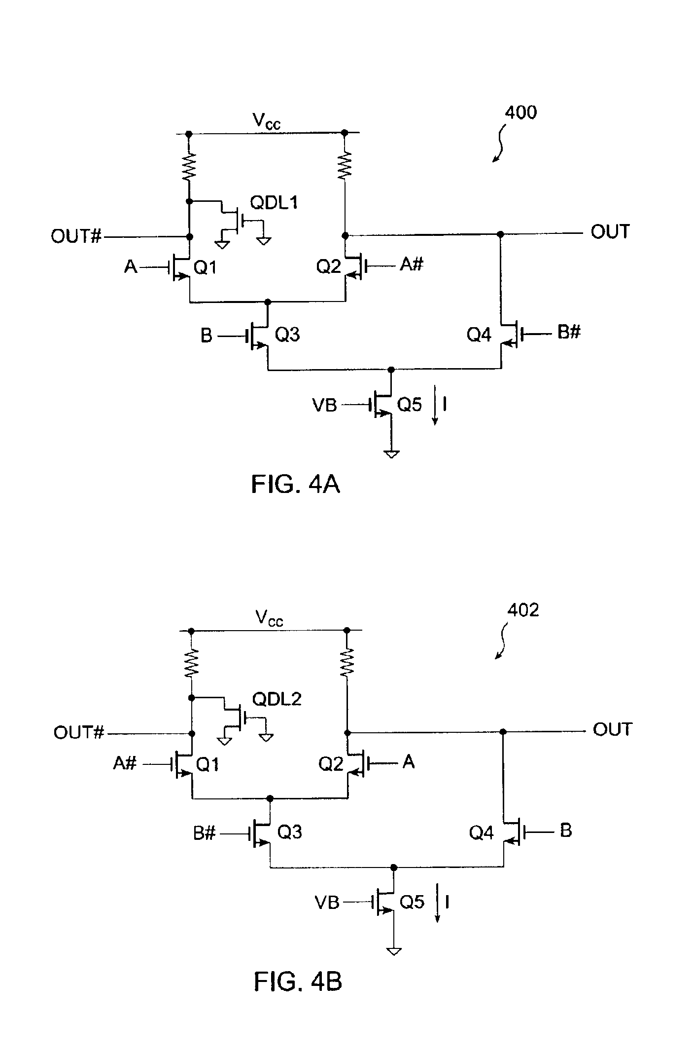
[0024]The present invention provides ultra high-speed logic circuitry implemented in silicon complementary metal-oxide-semiconductor (CMOS) process technology. A distinction is made herein between the terminology “CMOS process technology” and “CMOS logic.” CMOS process technology as used herein refers generally to a variety of well established CMOS fabrication processes that form a field-effect transistor over a silicon substrate with a gate terminal typically made of polysilicon material disposed on top of an insulating material such as silicon dioxide. CMOS logic, on the other hand, refers to the use of complementary CMOS transistors (n-channel and p-channel) to form various logic gates and more complex logic circuitry, wherein zero static current is dissipated. The present invention uses current-controlled mechanisms to develop a family of very fast current-controlled CMOS (or C3MOS™) logic that can be fabricated using a variety of conventional CMOS process technologies, but that...


PUM


Abstract

Various circuit techniques for implementing ultra high speed circuits use current-controlled CMOS (C3MOS) logic fabricated in conventional CMOS process technology. An entire family of logic elements including inverter/buffers, level shifters, NAND, NOR, XOR gates, latches, flip-flops and the like are implemented using C3MOS techniques. Optimum balance between power consumption and speed for each circuit application is achieve by combining high speed C3MOS logic with low power conventional CMOS logic. The combined C3MOS/CMOS logic allows greater integration of circuits such as high speed transceivers used in fiber optic communication systems.

Description

[0001]The present U.S. Utility Patent Application is a Continuation of U.S. patent application Ser. No. 09 / 484,856, filed Jan. 18, 2000, now U.S. Pat. No. 6,424,194 B1, which claims priority from U.S. Provisional Patent Application Ser. No. 60 / 141,355, filed Jun. 28, 1999, the disclosures of which are each incorporated herein by reference for all purposes.BACKGROUND OF THE INVENTION[0002]The present invention relates in general to integrated circuitry, and in particular to a complementary metal-oxide-semiconductor (CMOS) logic family with enhanced speed characteristics.[0003]For a number of reasons CMOS is the logic family of choice in today's VLSI devices. Due to the complementary nature of its operation, CMOS logic consumes zero static power. CMOS also readily scales with technology. These two features are highly desirable given the drastic growth in demand for low power and portable electronic devices. Further, with the computer aided design (CAD) industry's focus on developing a...

Claims


Application Information

Patent Timeline
Patent Type & Authority Patents(United States)
IPC IPC(8): H03K3/3562H03K3/356H03K19/094H03K17/693H03K3/00H03K19/21
CPCH03K3/356043H03K3/356139H03K3/3562H03K17/04163H03K17/693H03K19/09432H03K19/215H03K17/04106H03K17/04H03K2217/0036
Inventor HAIRAPETIAN, ARMOND
Owner AVAGO TECH INT SALES PTE LTD
Why Eureka
Try Eureka