Driving method of active matrix display device

a display device and active matrix technology, applied in the direction of electric digital data processing, instruments, computing, etc., can solve the problems of increasing the drive voltage of the driver, power consumption, power consumption, etc., and achieve the effect of preventing the influence of liquid crystal alignment and preventing the influence of image alignmen

Inactive Publication Date: 2005-06-28
SEMICON ENERGY LAB CO LTD
View PDF25 Cites 46 Cited by
  • Summary
  • Abstract
  • Description
  • Claims
  • Application Information

AI Technical Summary

Benefits of technology

[0029]Therefore, even if the potentials of the common lines vary, disorder in the alignment of the liquid crystal, and resulting influences on an image are prevented by making the absolute values of the potentials given to the common lines smaller than the threshold voltage of the liquid crystal.

Problems solved by technology

That is, although basically it is sufficient to apply a liquid crystal with effective voltages of a 5 V, the necessity of inversion requires a variation range of 10 V, i.e., +5 V to −5 V. This increases drive voltages of the driver, and hence is the greatest obstacle to reduction in power consumption.
There is another problem because of the increase of large potential variations of data, output potential differences (i.e., selection pulse heights) of the scan driver, and power consumption therein.
Further, due to large voltages applied to the active matrix circuit, the switching elements (transistors) will possibly be broken or their characteristics will possibly deteriorate.

Method used


Image

  • Driving method of active matrix display device
  • Driving method of active matrix display device
  • Driving method of active matrix display device

Examples


embodiment 1

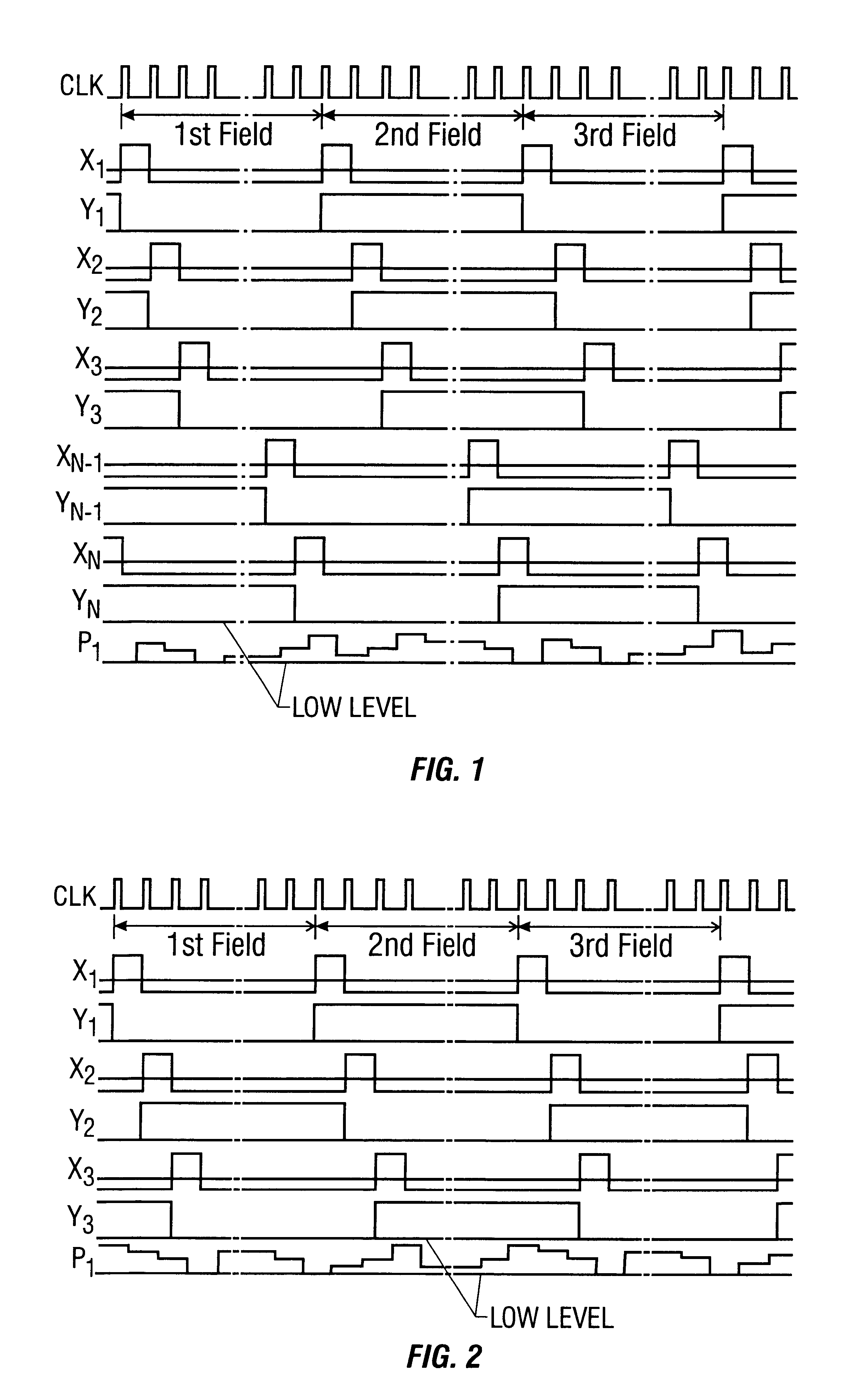
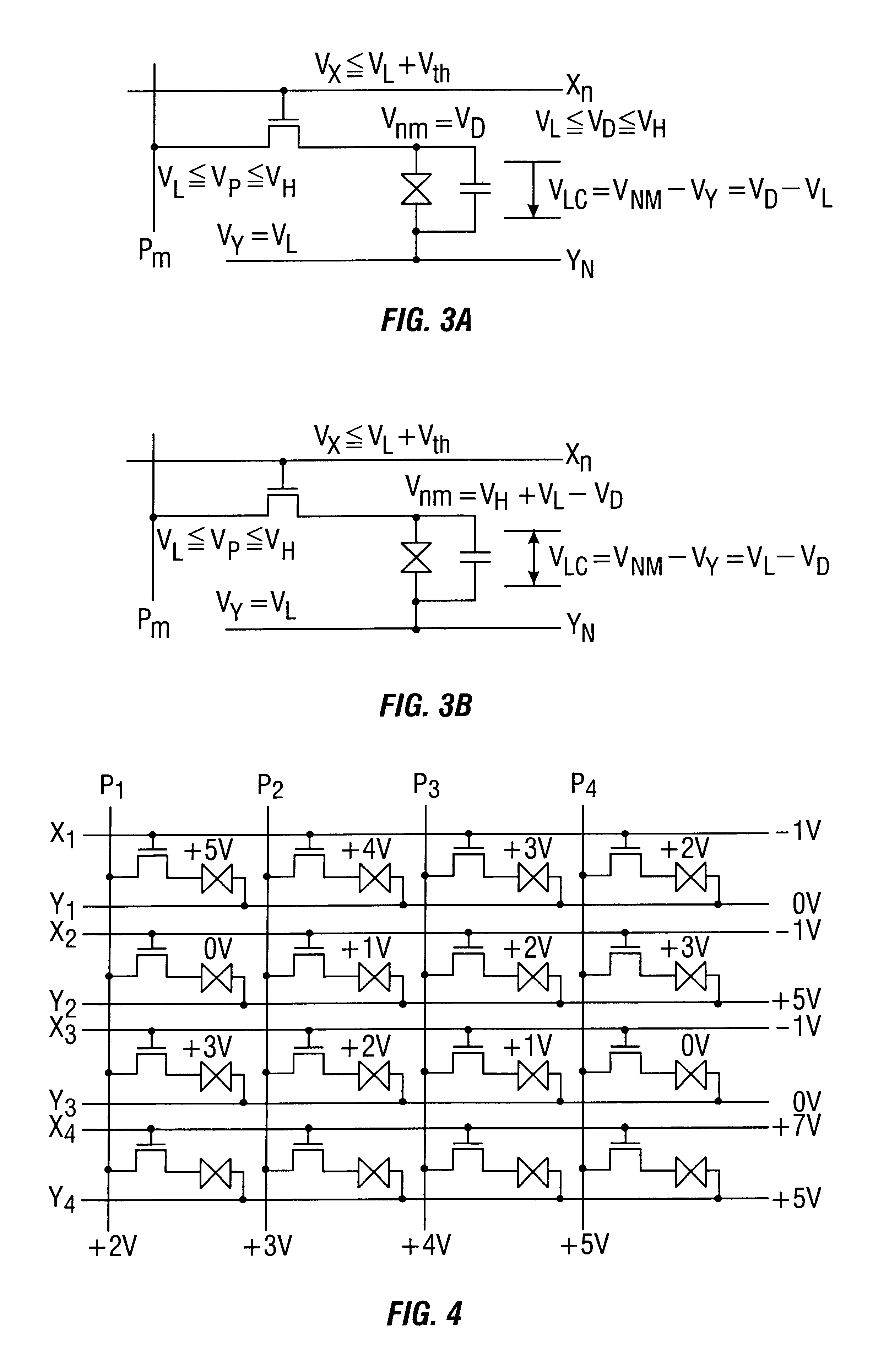
[0062]FIG. 1 shows a field inverting type driving method according to the invention in an N-row active matrix liquid crystal display device employing the IPS mode. In this embodiment, the same display data as shown in FIG. 8 are used. As shown in FIG. 1, in the first field, selection pulses are sequentially applied to N scan lines X1, X2, X3, . . . , XN-1, XN. At a time point when a pulse is applied to each scan line, the potential of the corresponding one of the common lines Y1, Y2, Y3, . . . , YN−1, YN decreases from the high-level (VH) to the low-level (VL). Thus, the state of FIG. 3A is realized.

[0063]Conversely, in the second field, when selection pulses are sequentially applied to the scan lines X1, X2, X3, . . . , XN−1, XN, the potentials of the corresponding common lines Y1, Y2, Y3, . . . , YN−1, YN increase from the low-level to the high-level. This the state of FIG. 3B is realized.

[0064]In the third field, the same operation as in the first field is performed. The directio...

embodiment 2

[0065]FIG. 2 shows a gate line inverting type driving method according to the invention in an N-row active matrix liquid crystal display device employing the IPS mode. As shown in FIG. 2, in the first field, the potentials of the odd-numbered common lines Y1, Y3, . . . are changed from the high-level to the low-level when selection pulses are applied to the corresponding scan lines. Conversely, the potentials of the even-numbered common lines Y2, Y4, . . . are changed from the low-level to the high-level when selection pulses are applied to the corresponding scan lines.

[0066]That is, in the first field, the state of FIG. 3A is established in the odd-numbered rows and the state of FIG. 3B is established in the even-numbered rows. Thus, a gate line inverting state is attained in which the directions of electric fields applied to the liquid crystal capacitor elements LC in adjacent rows are reverse to each other.

[0067]The operation in the second field is in converse to that in the firs...

embodiment 3

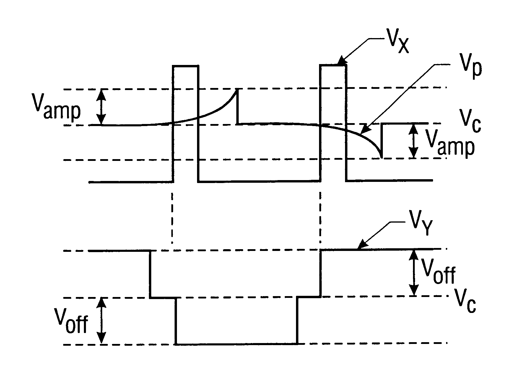
[0071]Differences between the driving method of the invention and the conventional driving method will be described below with reference FIGS. 11A-11C. FIGS. 11A-11C show waveforms of the potentials of the scan line Xn, the data line Pm, and the common line Yn that are connected to the pixel shown in FIG. 7. It is assumed that the field inverting scheme is employed. This embodiment employs a scheme in which an offset voltage Voff is always superimposed on the voltage that is applied to the pixel. In FIGS. 11A-11C, the potential VX applied to the scan line Xn and the potential VP of the data line Pm are expressed with overlapping on each other, the potential VY of the common line Vn is drawn separately with VC used as a reference potential when it varies over time (FIGS. 11B and 11C), to prevent the drawings from becoming unduly complex.

[0072]FIG. 11A shows the conventional driving method. The potential VY of the common line (or common electrode) Yn is kept at the constant value VC. ...


PUM


Abstract

In a liquid crystal display device of the in-plane switching mode (IPS mode), the potential of data that is output from a data driver is set at values between potentials that are given to common lines. Two levels, i.e., high and low levels, are prepared for the potential to be given to the common lines and the potential is inverted between those levels in every field, whereby the polarity of a voltage between both electrodes of a pixel is inverted. As a result, the potential variation ranges of signals that are output from the data driver and a scan driver can be greatly reduced from those of the conventional case, which contributes to reduction in the power consumption of the drivers. Since the voltage applied to a switching element for controlling each pixel can be reduced, the load of the switching element can also be reduced.

Description

[0001]This is a continuation of U.S. application Ser. No. 08 / 823,238, filed Mar. 24, 1997 now U.S. Pat. No. 5,847,687.BACKGROUND OF THE INVENTION[0002]1. Field of the Invention[0003]The present invention relates to an active matrix display device. In particular, the invention relates to an active matrix display device which employs a display method of the in-plane switching mode (also called IPS mode). The invention is intended to reduce potential variation of signals (or data) to thereby lower the power consumption, and to reduce voltages applied to the switching elements that are provided for the respective pixels to thereby lower the loads of the switching elements. The invention also relates to a driving method of a capacitive-coupling-type display device such as a liquid crystal display device.[0004]2. Description of Related Art[0005]In a capacitive-coupling-type display device such as a liquid crystal display device, it is necessary to invert the polarity of a voltage applied ...

Claims


Application Information

Patent Timeline
Patent Type & Authority Patents(United States)
IPC IPC(8): G09G3/36
CPCG09G3/3614G09G3/3648G09G3/3659G09G3/3655G09G2330/04G09G2300/0434G09G2330/025
Inventor HIRAKATA, YOSHIHARUTAKEMURA, YASUHIKO
Owner SEMICON ENERGY LAB CO LTD
Why Eureka
Try Eureka