
Line selector for a matrix of memory elements

a memory element and selector technology, applied in the field of semiconductor memories, can solve the problems of increased erase time and power consumption, unnecessary stress on memory cells, and worsening the situation

Inactive Publication Date: 2005-08-16
MICRON TECH INC
View PDF11 Cites 20 Cited by
  • Summary
  • Abstract
  • Description
  • Claims
  • Application Information

AI Technical Summary

Problems solved by technology

This causes an unnecessary stress on the memory cells.
In electrically erasable memories having memory cells formed by MOS transistors with a conductive floating gate, the memory cells may enter a depletion condition, which typically needs to be recovered by re-writing the memory cells; the erase time and the power consumption are, thus, increased.
The situation is even worse in the case of memories having memory cells formed by MOS transistors with a charge-trapping layer, typically of silicon nitride (such as the transistors exploited for forming dual-bit memory cells).

Method used


Image

  • Line selector for a matrix of memory elements
  • Line selector for a matrix of memory elements
  • Line selector for a matrix of memory elements

Examples


Embodiment Construction

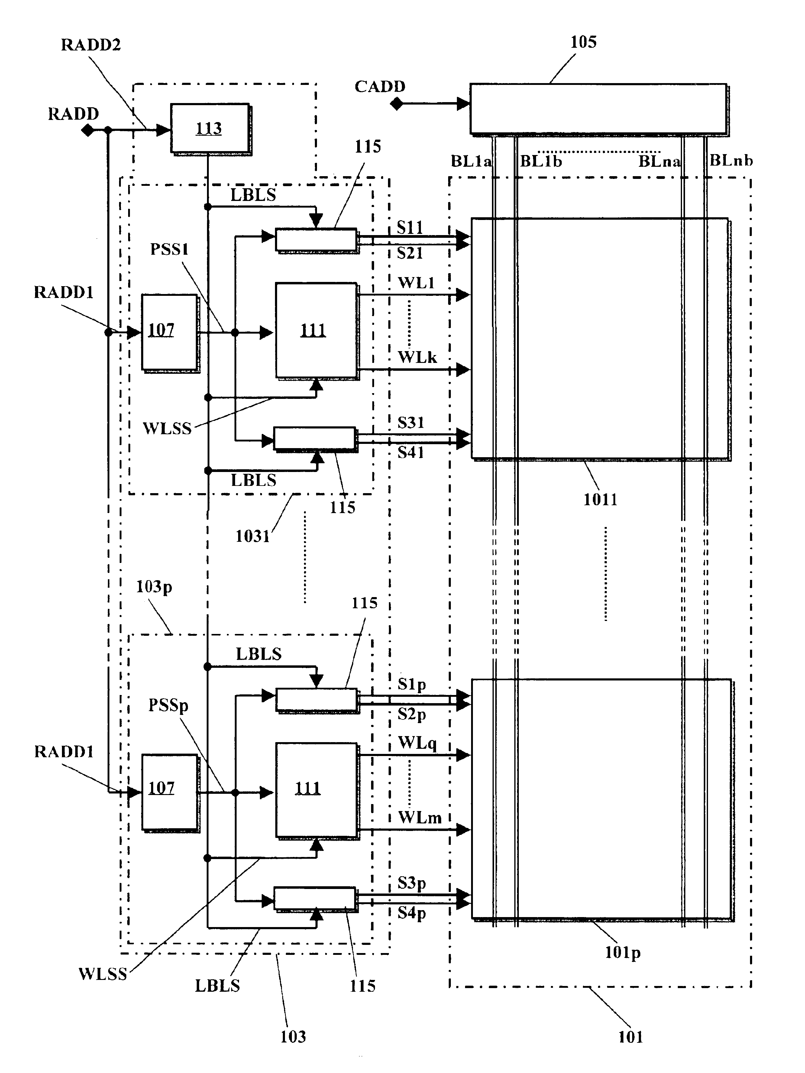
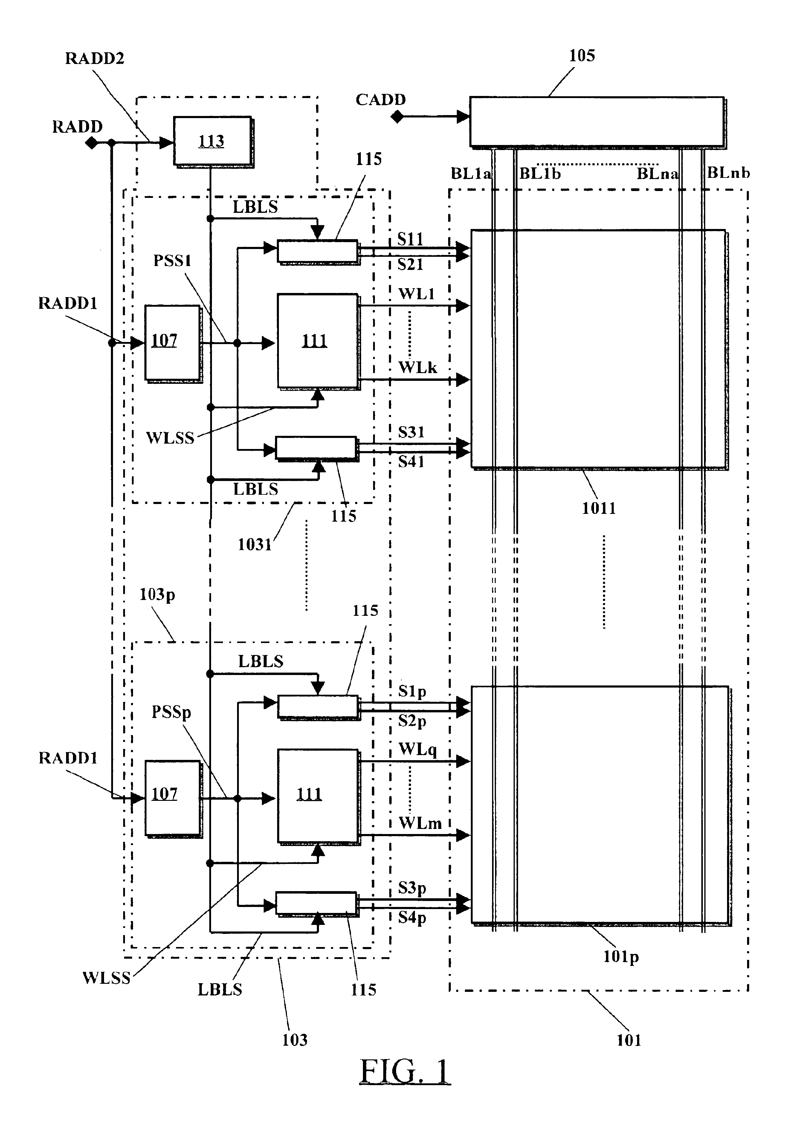
[0029]Referring to the drawings, FIG. 1 shows schematically the relevant circuit blocks of an electrically erasable and programmable memory having a word line selector according to an embodiment of the present invention. In particular, and by way of example only, a memory with dual-bit memory cells is considered, i.e., a memory in which the memory cells are capable of storing two bits in two different charge-storage areas of a charge-trapping layer (typically made of silicon nitride). This is, however, not to be intended as a limitation of the present invention, which can be applied to different types of electrically erasable and programmable memories, and particularly to Flash memories having memory cells with a conductive floating gate.

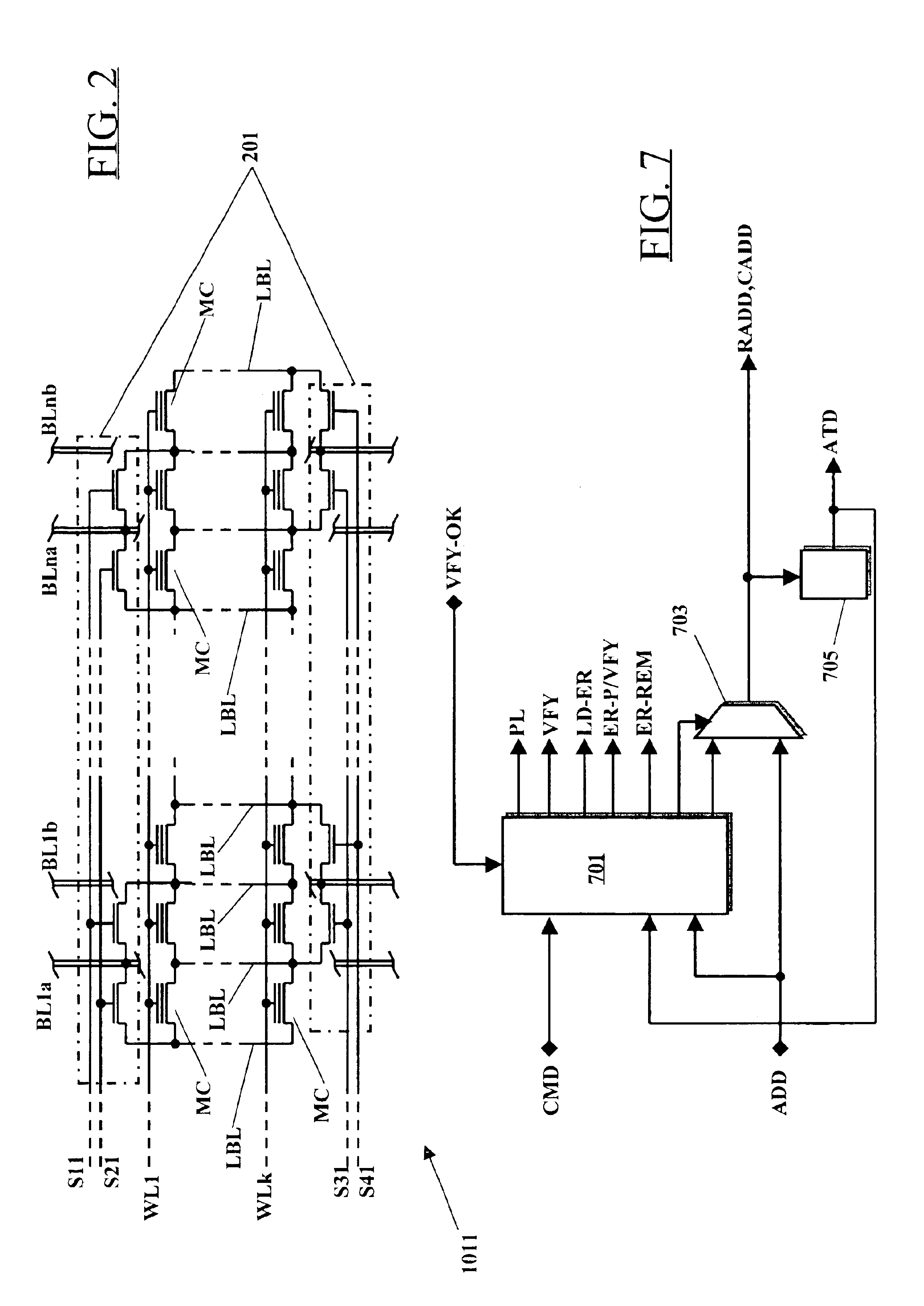
[0030]The memory comprises a matrix 101 of memory cells (each memory cell being identified by MC in FIG. 2), arranged by rows and columns.

[0031]The memory cells belonging to a same matrix row are connected to a same word line of a plurality of word ...


PUM


Abstract

A line selector for a matrix of memory elements, for example a word line selector, comprises a plurality of line group selection circuits, each one allowing the selection of a respective group of matrix lines according to an address; each matrix line group includes at least one matrix line. Flag means are associated with each line group, that can be set to declare a pending status of a prescribed operation, for example an erase operation, for the respective matrix line group. Means are provided for entrusting the flag means with the selection of the respective line group during the execution of the prescribed operation, in alternative to the respective line group selection circuit. The flag means enable, when set, the execution of the prescribed operation on the respective matrix line group.

Description

PRIORITY CLAIM[0001]This application claims priority from European patent application No. 02425453.4, filed Jul. 10, 2002, which is incorporated herein by reference.[0002]1. Technical Field[0003]The present invention generally relates to the field of semiconductor memories, particularly, but not exclusively, to non-volatile memories and even more particularly to non-volatile electrically erasable memories.[0004]2. Background of the Invention[0005]An important feature of non-volatile electrically erasable (and programmable) memories is the reliability towards multiple write / erase cycles.[0006]Similar to a write operation, an erase operation is normally carried out in a plurality of steps; each step provides for applying an erase pulse to the memory cells to be erased, and then verifying whether the memory cells have been erased or an additional erase pulse is required.[0007]Normally, in a memory, some memory cells are erased faster than others. While some memory cells require few era...

Claims


Application Information

Patent Timeline
IPC IPC(8): G11C8/00G11C8/12G11C16/08G11C16/06G11C16/16G11C8/02
CPCG11C8/12G11C16/08G11C16/16
Inventor PASCUCCI, LUIGI
Owner MICRON TECH INC
Learn More