
High efficiency redundancy architecture in SRAM compiler

a compiler and high-efficiency technology, applied in the field of integrated circuits, can solve the problems of reducing the need for such high-efficiency redundancy, affecting the timing performance, and faults within the memory circuit, so as to achieve the effect of minimally affecting timing performan

Inactive Publication Date: 2005-08-16
TAIWAN SEMICON MFG CO LTD
View PDF14 Cites 5 Cited by
  • Summary
  • Abstract
  • Description
  • Claims
  • Application Information

AI Technical Summary

Benefits of technology

The invention provides a yield enhancement circuit that can replace a defective circuit with a redundant circuit while minimizing the impact on timing performance. The circuit has multiple fault indication devices that detect the presence of a fault in a sub-circuit of an integrated circuit and activate a fault detection device to determine the existence of a fault. A redundancy activation circuit is then activated to transfer input / output signals to a designated path dependent on the expression of the fault. The circuit can be used in memory and other types of integrated circuits. The technical effect of the invention is to improve the reliability and yield of integrated circuits.

Problems solved by technology

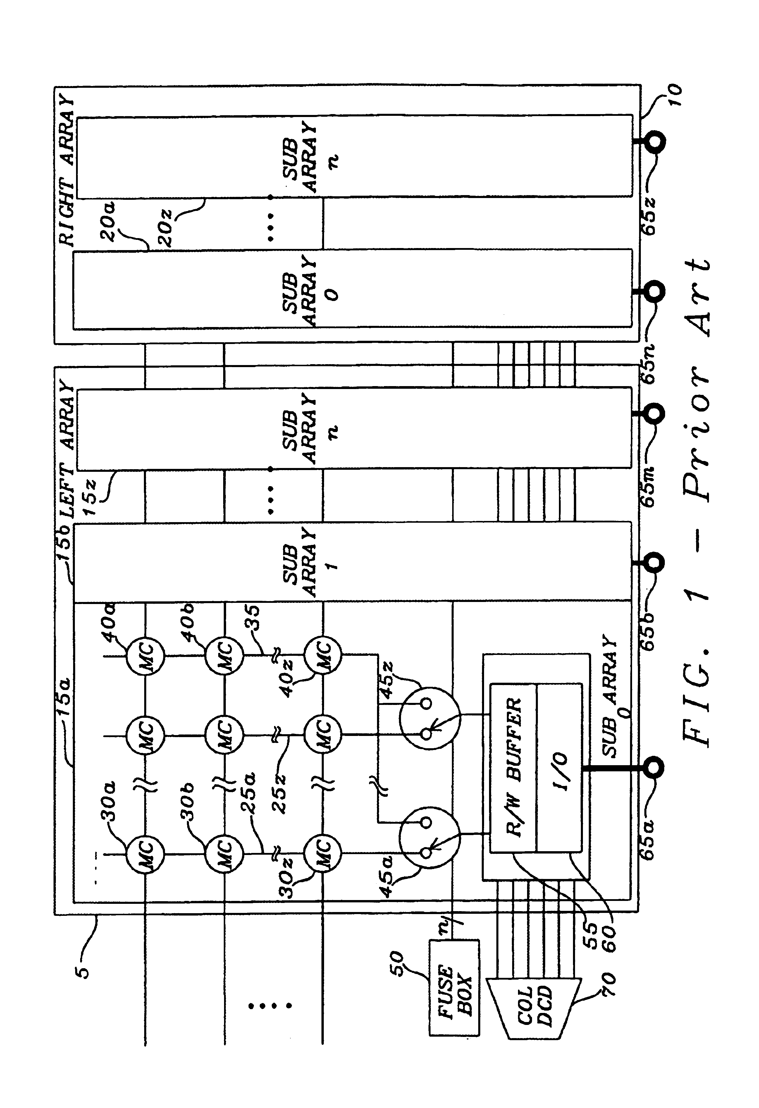
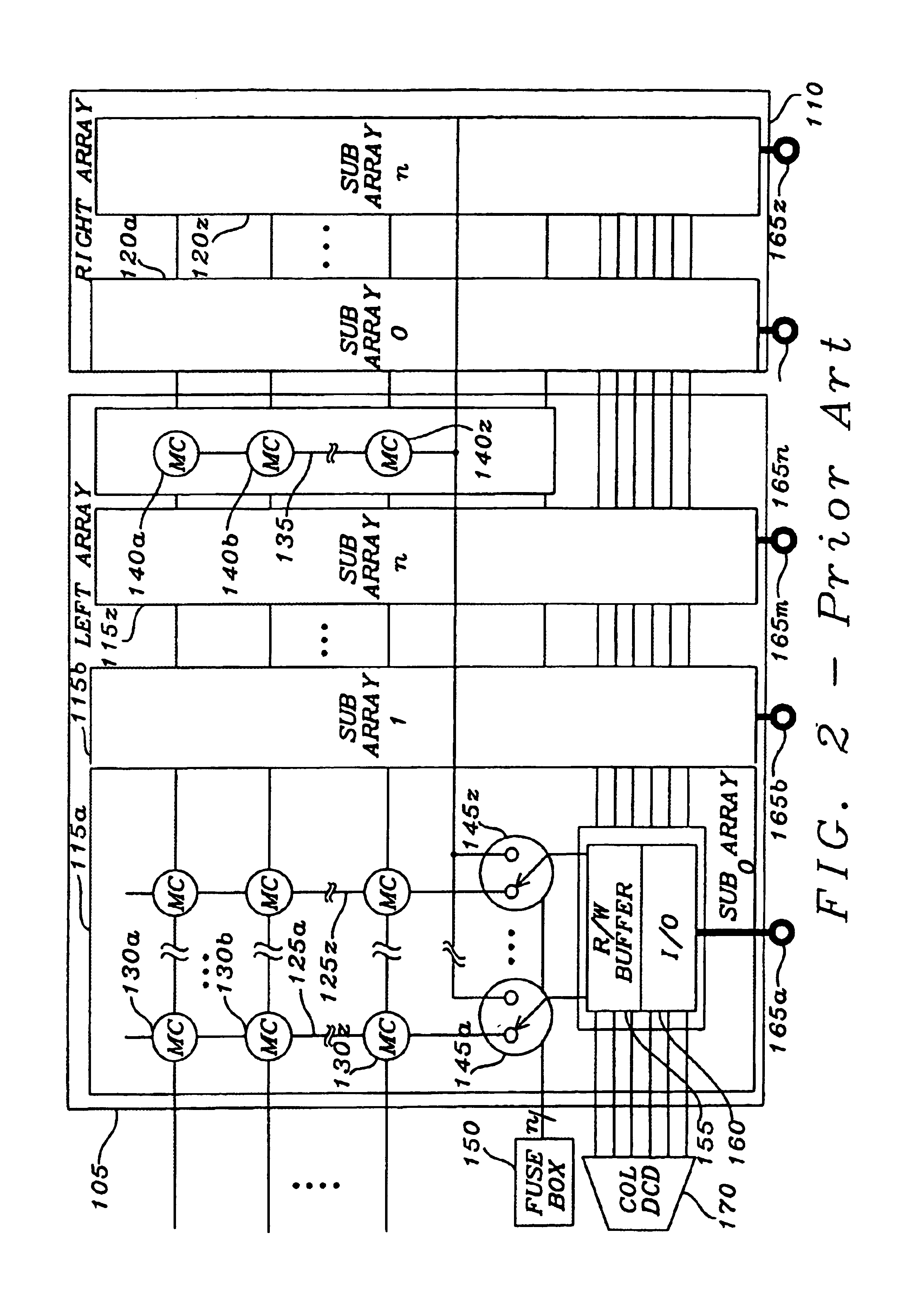
In the processing of the memory circuits, contamination or defects within the process will cause faults within the memory circuit.
This organization places a large overhead in space for the redundancy.
As process techniques have improved, contamination and defects have decreased, thus ameliorating the need for such high levels of redundancy.
The wiring to connect the redundant column of memory cells so that it can be connected within the array or arrays is relatively long and affects the performance of the memory.

Method used


Image

  • High efficiency redundancy architecture in SRAM compiler
  • High efficiency redundancy architecture in SRAM compiler
  • High efficiency redundancy architecture in SRAM compiler

Examples


Embodiment Construction

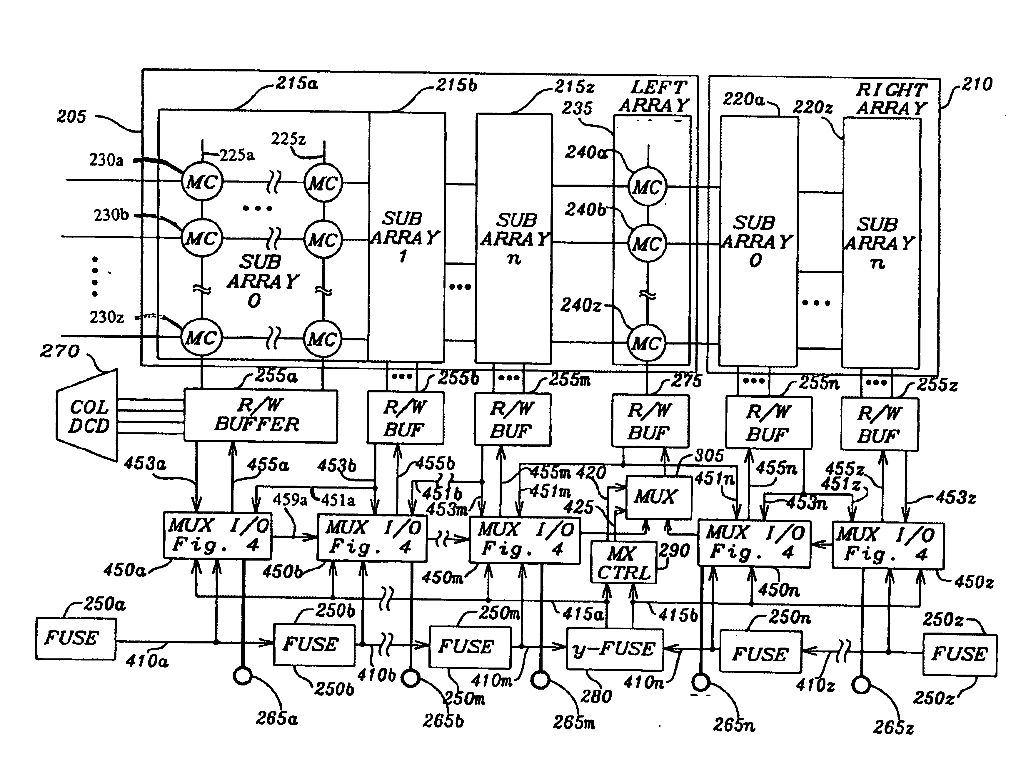
[0037]The memory circuit of this invention is particularly suited (but not exclusively) to SRAM that is embedded with other circuitry in an integrated circuit. The memory circuit of this invention incorporates an architecture that permits a single redundant column of memory cells and minimizes the effects of the interconnection wiring of the redundant column on the performance of the memory. The single redundant column of memory cells is placed relatively central to the placement of the arrays of memory cells for which the redundant column is to provide yield enhancement protection.

[0038]A fault indication device is associated with each column of the arrays of memory cells. Generally, the fault indication device has a fuse that is destroyed if the associated column of memory cells has a fault. This causes a fault signal that is transmitted to selected adjacent fault indication devices. The fault indication device has a combinational logic circuit such as an OR gate that combines the...


PUM


Abstract

A yield enhancement circuit substitutes a redundant sub-circuit for a faulty sub-circuit in an integrated circuit such as memory. The yield enhancement circuit has a plurality of fault indication devices, which is associated with one sub circuit of the integrated circuits such that one fault indication device is activated to generate a fault signal to express the existence of a fault within the faulty sub-circuit. Additionally selected adjacent fault indication devices generate the fault signal to express the existence of the fault within the faulty circuit. A fault detection device determines the existence of the faulty sub-circuit and transmits a redundancy implementation signal to a plurality of redundancy activation circuits. Each redundancy activation circuit selectively transfers input / output signals to a designated path dependent on the expression of the existence of a fault within the integrated circuit.

Description

BACKGROUND OF THE INVENTION[0001]1. Field of the Invention[0002]This invention relates generally to integrated circuits and more particularly to yield enhancement circuits by implementing redundant sub-circuits for faulty sub-circuits of the integrated circuits. Even more particularly this invention relates to yield enhancement circuits for substituting redundant columns of memory cells for faulty columns of memory cells in memory arrays such as static random access memory (SRAM).[0003]2. Description of Related Art[0004]Yield enhancement circuitry for integrated circuits, particularly for memory integrated circuits, is well known in the art. Memory integrated circuits are formed of multiple arrays of memory cells. Each memory array is constructed of rows and columns of memory cells. Normally, the rows of memory cells are selected by an address decoder. The columns of memory cells are bounded by read / write buffers that retrieve data from and store data to the selected memory cell. A ...

Claims


Application Information

Patent Timeline
Patent Type & Authority Patents(United States)
IPC IPC(8): G11C7/00G11C29/00
CPCG11C29/848
Inventor WANG, TAO-PING
Owner TAIWAN SEMICON MFG CO LTD
Learn More