

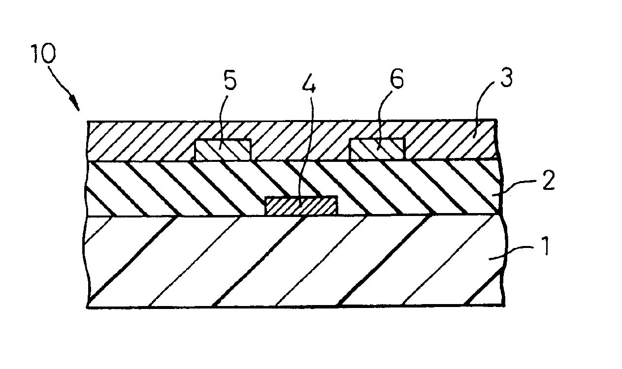
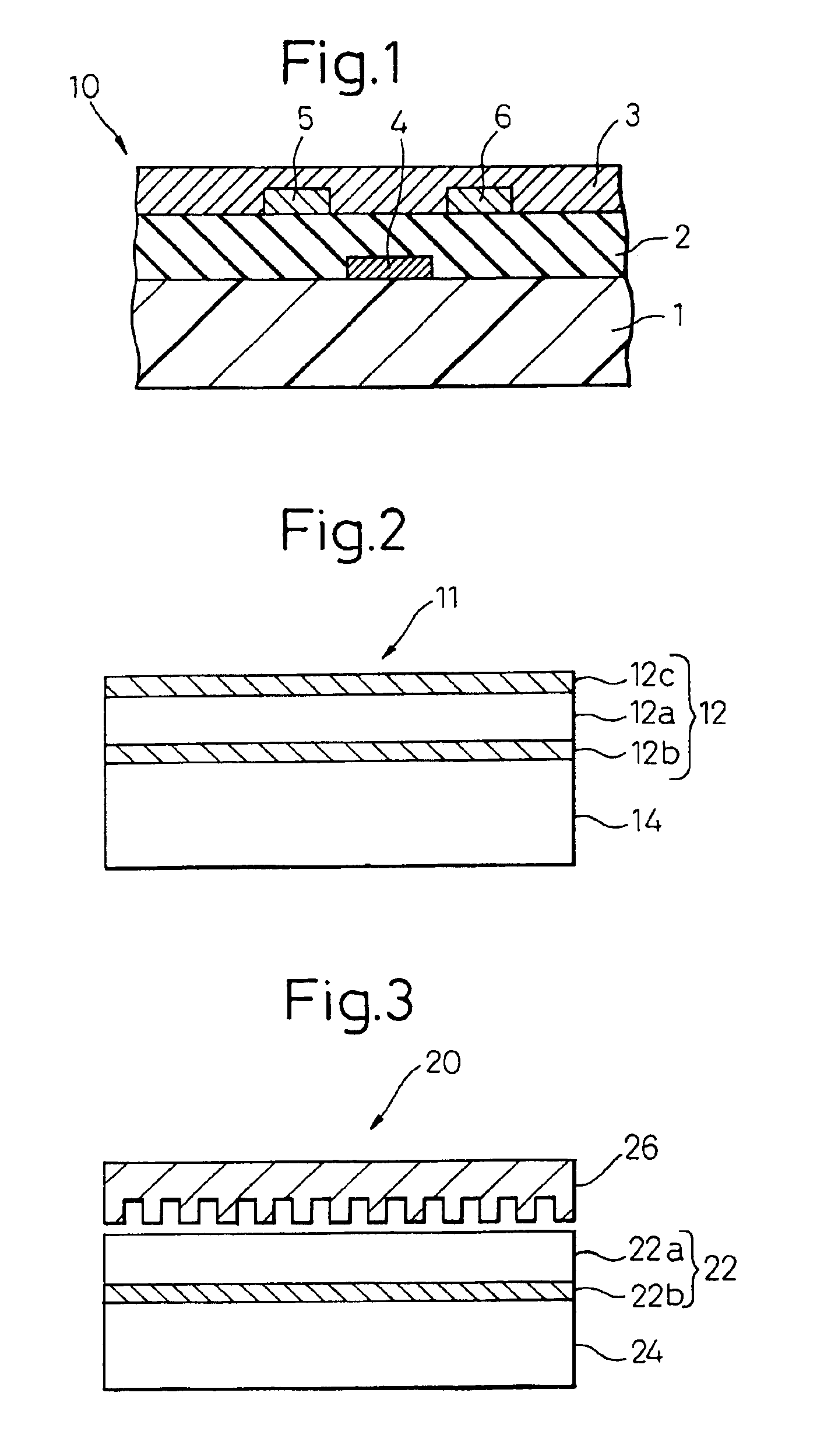
Electrically conducting organic compound and electronic device
- Summary
- Abstract
- Description
- Claims
- Application Information
AI Technical Summary
Benefits of technology
Problems solved by technology
Method used
Image

Examples
examples of form
[0117]From A4 to A3 size (foldable into A4 size), slightly foldable board, and attachable / detachable to wall, etc.
Examples of Function:
[0118]Receiving and sending, data memory, switchover of picture plane, enlargement / reduction, input, individualization of parts (constituent element), signal display, etc.
Examples of Constituent Element:
[0119]Display part, driving circuit, power source, communication (sending and receiving) circuit, control circuit, memory, input means, signal display means, etc.
Examples of Application:
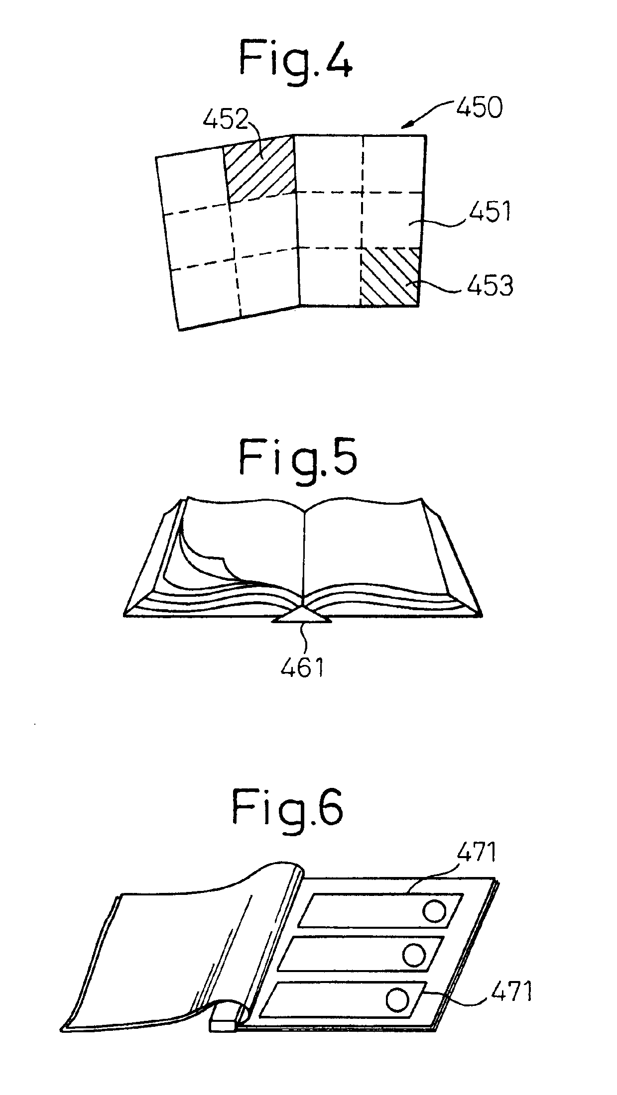
[0120]FIGS. 7A and 7B show the appearance of a display board system 480. A system having respective means for terminal connection, receiving and sending, data memory, switchover of picture plane, enlargement / reduction and input is provided on a wall. In the portion 481 fixed to the wall, a communication circuit and signal means (not shown) is provided, a display and input part 482 having provided therein a driving circuit, a control circuit, a power source and the like...
example 1
[0235]On a substrate plastic sheet comprising polyether sulfone, a gate electrode was formed by sputtering of gold, cyanoethylated pullulan dissolved in acetone was coated thereon, and then the solvent was dried to form an insulating layer having a film thickness of 150 nm. On this insulating layer, a source electrode and a drain electrode at an electrode-to-electrode distance, namely, a channel length, of 5 μm were each formed to a film thickness of 50 nm by sputtering of gold. On the plastic substrate with electrodes thus formed, an ovalene derivative having attached thereto a hexyl group (see, the following formula):
which was dissolved under heating in toluene was coated by spin coating and then, the solvent was gradually dried to obtain a channel layer having a film thickness of 100 nm.
[0236]Subsequently, for the thus-manufactured organic thin film transistor, the mobility of the electrically conducting organic compound was calculated from the relationships between the drain vo...
example 2
[0237]On a substrate plastic sheet comprising polyether sulfone, a gate electrode was formed by sputtering of gold and patterning, cyanoethylated pullulan dissolved in acetone was coated thereon, and then the solvent was dried to form an insulating layer having a film thickness of 150 nm. On this insulating layer, a source electrode and a drain electrode at an electrode-to-electrode distance, namely, a channel length, of 5 μm were formed each to a film thickness of 50 nm by sputtering of gold.
[0238]On the plastic substrate with electrodes thus formed, a bianthrene derivative having attached thereto a hexyl group (see, the following formula):
which was dissolved under heating in toluene was coated by spin coating and then, the solvent was gradually dried while applying an electric field between the source-drain electrodes to obtain a channel layer having a film thickness of 100 nm.
[0239]Subsequently, for thus-manufactured organic thin film transistor, the mobility of the electrically...
PUM
| Property | Measurement | Unit |
|---|---|---|
| Area | aaaaa | aaaaa |
| Flexibility | aaaaa | aaaaa |
| Molecular weight | aaaaa | aaaaa |
Abstract
Description
Claims
Application Information