

Semiconductor memory device and electronic device for activation control of word lines in a semiconductor memory device
a technology of semiconductor memory and activation control, which is applied in the direction of information storage, static storage, digital storage, etc., can solve the problem of shortening the time elapse before the start of a read access, and achieve the effect of removing the long rate restriction of a semiconductor memory devi
- Summary
- Abstract
- Description
- Claims
- Application Information
AI Technical Summary
Benefits of technology
Problems solved by technology
Method used
Image

Examples
Embodiment Construction
[0033]One mode of carrying out the invention is discussed below as a preferred embodiment in the following sequence:[0034]A. Terminal Structure of Semiconductor Memory Device and Outline of Working State[0035]B. Internal Structure of Semiconductor Memory Device[0036]B1. General Structure[0037]B2. Row Control Circuit[0038]B.2.1 Read Execution Signal Generator[0039]B.2.2 Write Execution Signal Generator[0040]B.2.3 Refresh Execution Signal Generator[0041]B.2.4 Operations of Respective Generators[0042]B3. Address Buffer and Data Input Buffer[0043]B.3.1 Address Buffer[0044]B.3.2 Data Input Buffer[0045]C. Operations in Operation Mode[0046]C1. Read Access[0047]C2. Early Write Access[0048]C3. Delay Write Access[0049]D. Application to Electronic Device[0050]E. Modification
A. Terminal Structure of Semiconductor Memory Device and Outline of Working State
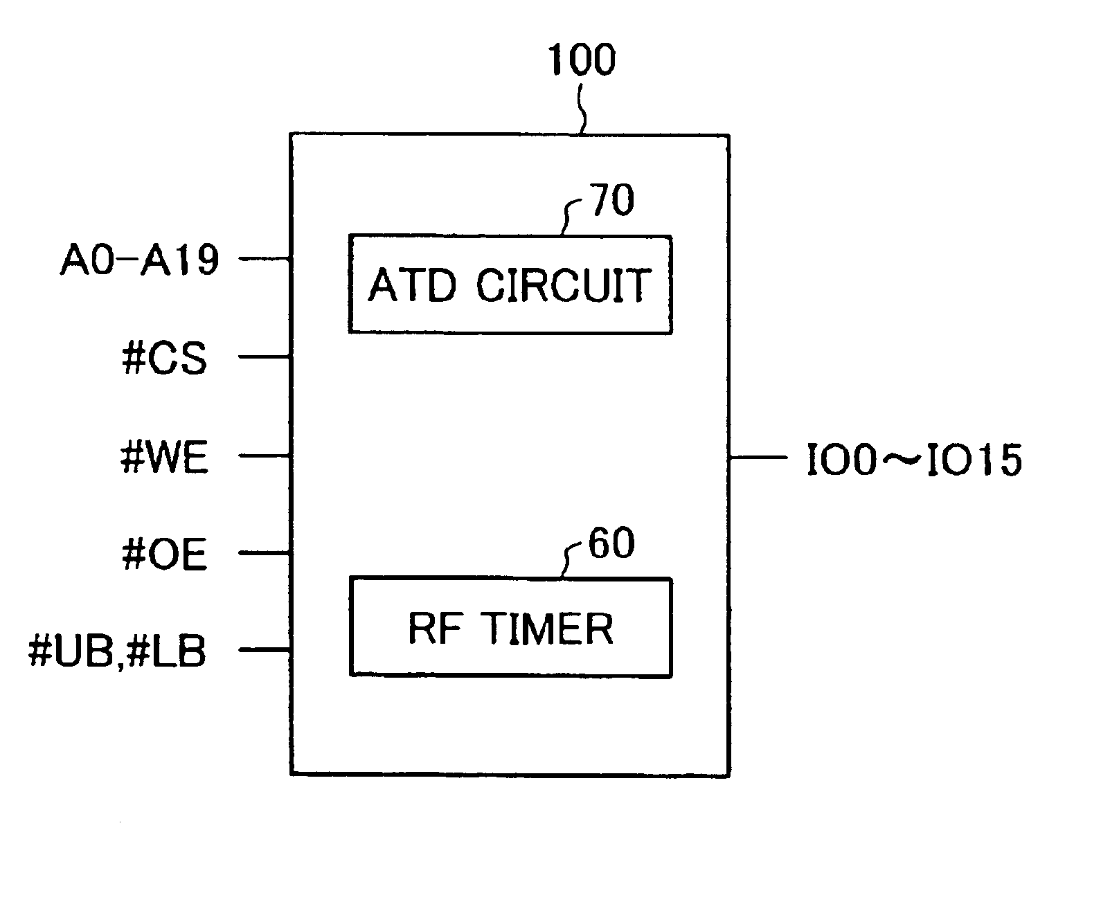
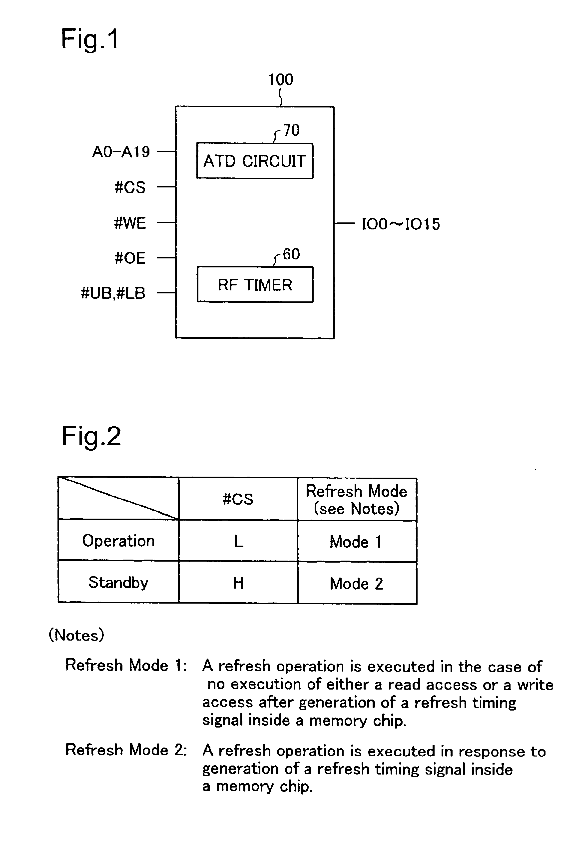
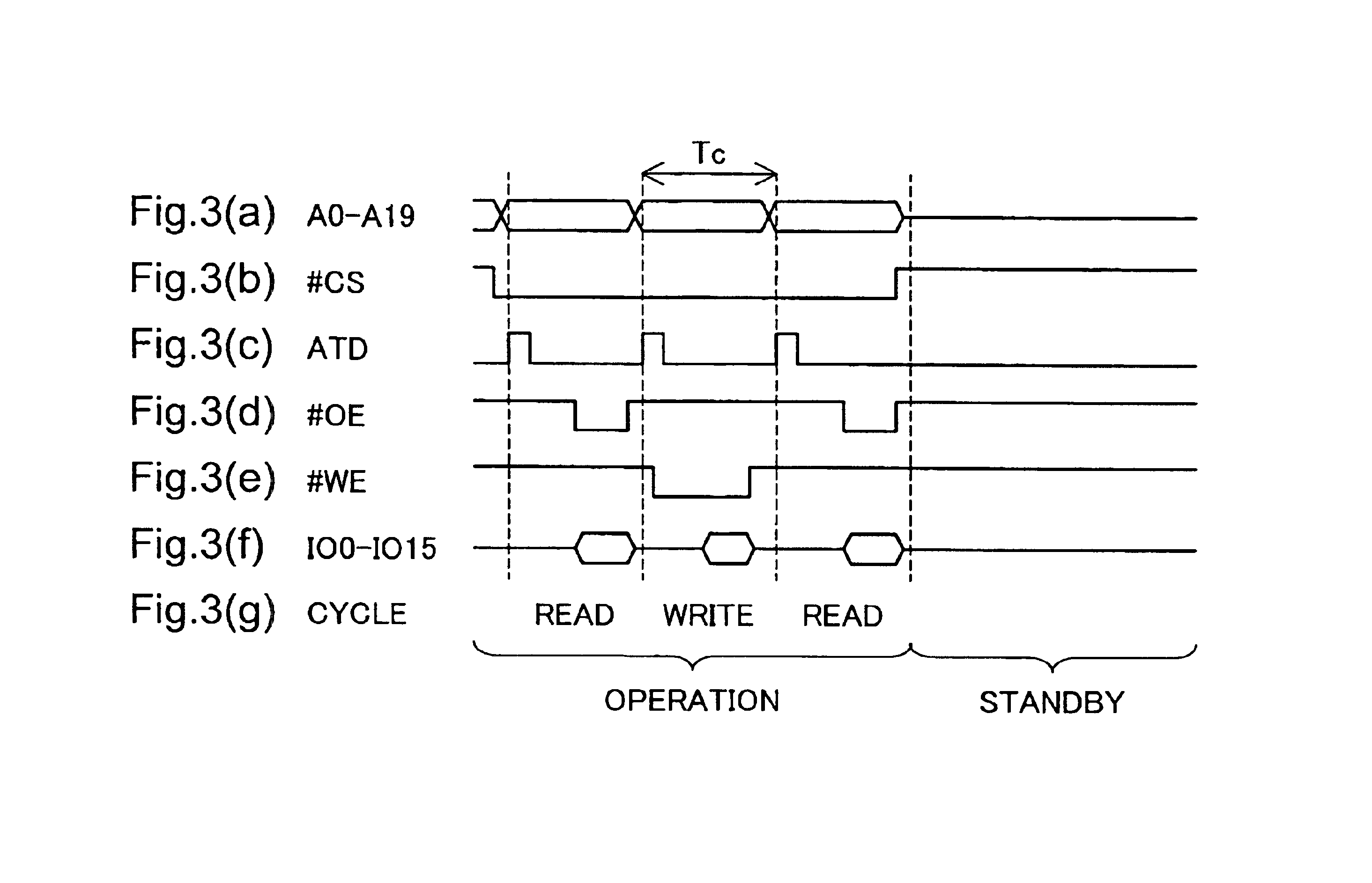
[0051]FIG. 1 shows the terminal structure of a memory chip 100 in one embodiment of the semiconductor memory device of the invention. The memo...
PUM
 Abstract
Description
Claims
Application Information