Liquid crystal display device

a liquid crystal display and display device technology, applied in non-linear optics, instruments, optics, etc., can solve the problems of narrow viewing angle of conventional twist nematic and super twist nematic liquid crystal display devices, difficult to realize stable production of devices, and high probability of rubbing streaks in displayed images, etc., to achieve wide viewing angle and high display quality.

Inactive Publication Date: 2005-11-15
SHARP KK
View PDF22 Cites 43 Cited by
  • Summary
  • Abstract
  • Description
  • Claims
  • Application Information

AI Technical Summary

Benefits of technology

[0011]The present invention has been made to solve the problem in the prior art, and has an object to provide a liquid crystal display device having a wide viewing angle characteristic and a high display quality.

Problems solved by technology

However, conventional twist nematic (TN) type and super twist nematic (STN) type liquid crystal display devices have a narrow viewing angle.
While the transverse electric field mode is an effective approach to improve the viewing angle, the production process thereof imposes a significantly lower production margin than that of a normal TN type device, whereby it is difficult to realize stable production of the device.
However, when a vertical alignment film is subjected to a rubbing treatment, rubbing streaks are likely to appear in the displayed image, and it is not suitable for mass-production.
However, the present inventors reviewed these publications and found that with the methods disclosed therein, the orientation in regions of the liquid crystal layer corresponding to the openings in the electrode is not defined, whereby the orientation of the liquid crystal molecules is not sufficiently continuous, and it is difficult to achieve a stable orientation across each pixel, resulting in a display with non-uniformity.
However, the present inventors have found that the display quality may not be improved sufficiently only by providing an electrode structure as disclosed in this patent application.

Method used


Image

  • Liquid crystal display device
  • Liquid crystal display device
  • Liquid crystal display device

Examples


Embodiment Construction

[0103]Embodiments of the present invention will now be described with reference to the drawings.

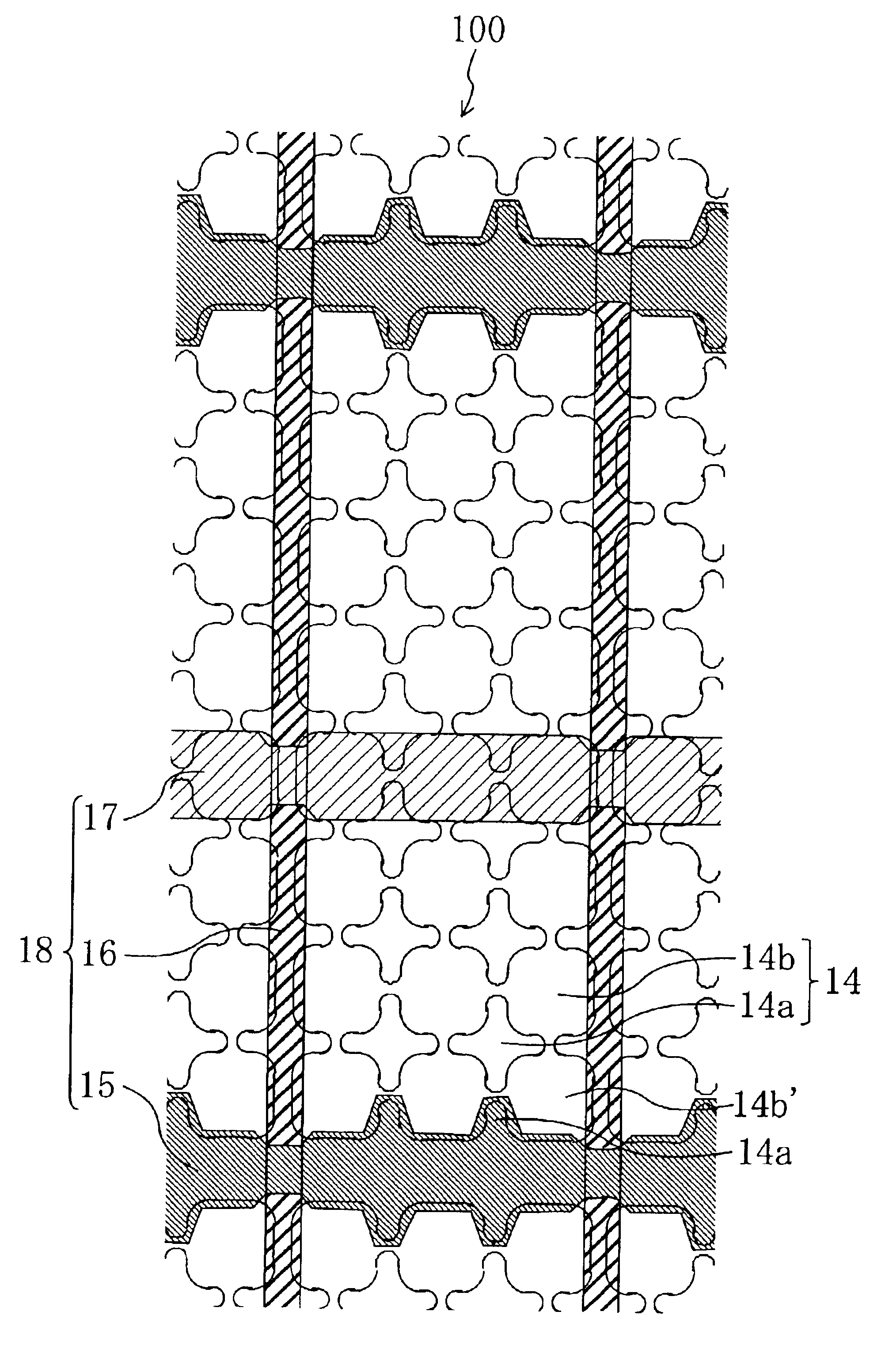
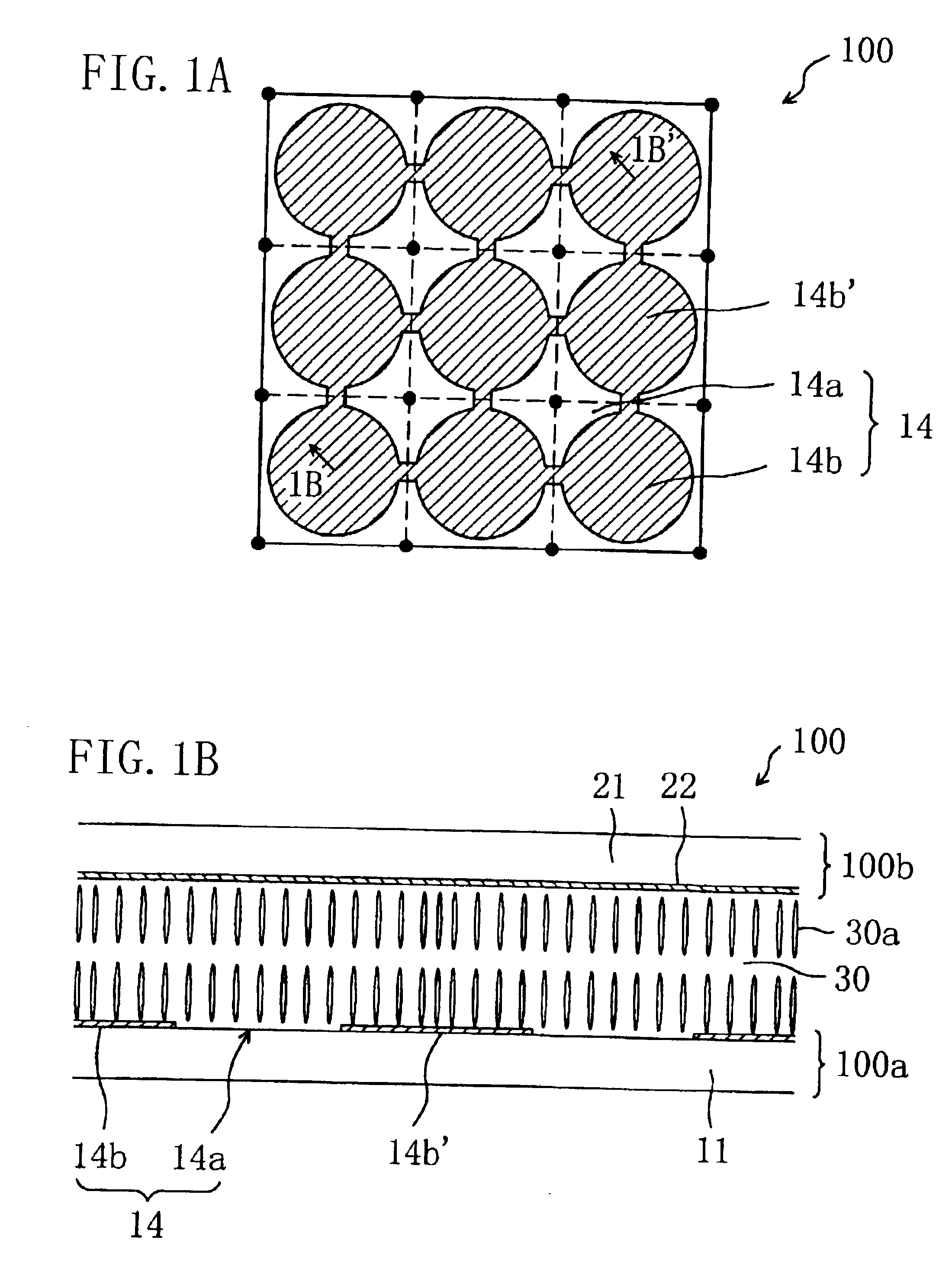
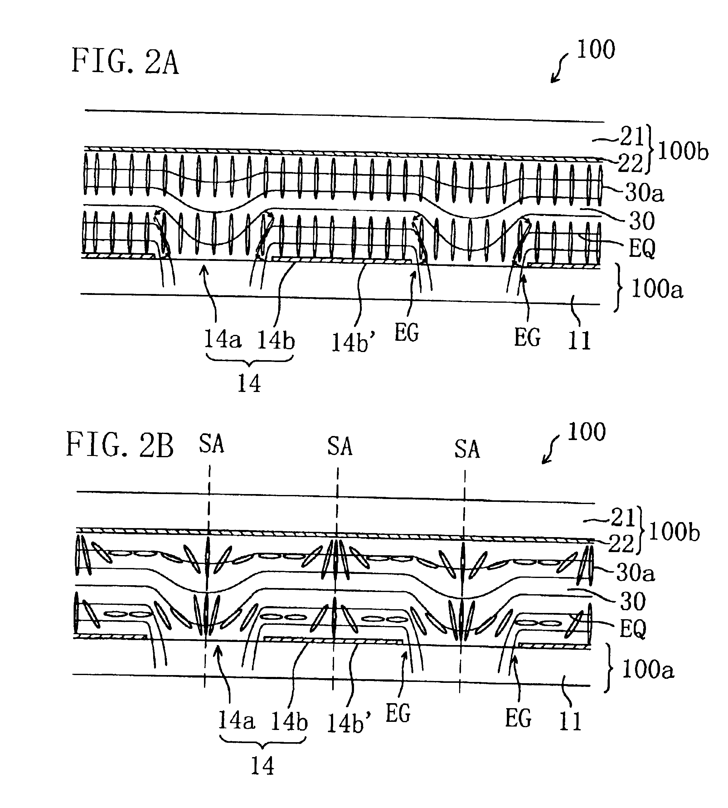
[0104]First, the electrode structure of the liquid crystal display device of the present invention and the function thereof will be described. The preferred embodiments of the present invention will be hereinafter described with respect to an active matrix type liquid crystal display device using thin film transistors (TFTs). Moreover, while the preferred embodiments of the present invention will be described with respect to a transmission type liquid crystal display device, the present invention can alternatively be used with a reflection type liquid crystal display device or a transmission / reflection combination type liquid crystal display device.

[0105]Note that in the present specification, a region of a liquid crystal display device corresponding to a “picture element”, which is the minimum unit of display, will be referred to as a “picture element region”. In a color liquid crystal d...


PUM

PropertyMeasurementUnit
angleaaaaaaaaaa
widthaaaaaaaaaa
diameteraaaaaaaaaa

Abstract

A first substrate includes, on one side thereof that is closer to a liquid crystal layer, a picture element electrode provided for each picture element region, a switching element, and a bus line. A second substrate includes a counter electrode opposing the picture element electrode. The picture element electrode includes a plurality of openings and a solid portion that includes a plurality of unit solid portions. In each picture element region, the liquid crystal layer takes a vertical alignment in the absence of an applied voltage, and forms a plurality of liquid crystal domains, each of which takes a radially-inclined orientation, in the plurality of openings and the solid portion by inclined electric fields produced at respective edge portions of the plurality of openings of the picture element electrode in response to an applied voltage. In each picture element region, at least one of the plurality of openings of the picture element electrode that is located along the bus line and located between two adjacent ones of the plurality of unit solid portions is superposed on the bus line.

Description

BACKGROUND OF THE INVENTION[0001]1. Field of the Invention[0002]The present invention relates to a liquid crystal display device, and more particularly to a liquid crystal display device having a wide viewing angle characteristic and being capable of producing a high quality display.[0003]2. Description of the Background Art[0004]In recent years, liquid crystal display devices, which are thin and light in weight, are used as personal computer displays and PDA (personal digital assistance) displays. However, conventional twist nematic (TN) type and super twist nematic (STN) type liquid crystal display devices have a narrow viewing angle. Various technical developments have been undertaken to solve the problem.[0005]A typical technique for improving the viewing angle characteristic of a TN or STN type liquid crystal display device is to add an optical compensation plate thereto. Another approach is to employ a transverse electric field mode in which a horizontal electric field with re...

Claims


Application Information

Patent Timeline
Patent Type & Authority Patents(United States)
IPC IPC(8): G02F1/1337G02F1/1343G02F1/13G02F1/1333G02F1/139
CPCG02F1/133707G02F1/1393G02F1/134309
Inventor KUBO, MASUMIOGISHIMA, KIYOSHIOCHI, TAKASHIWATANABE, KEIZOH
Owner SHARP KK
Why Eureka
Try Eureka