Input/output coupling structure for dielectric waveguide resonator

a dielectric waveguide and coupling structure technology, applied in the direction of coupling devices, resonators, electrical equipment, etc., can solve the problems of poor mass-productivity and considerable difficulty in forming input/output electrode patterns, and achieve the effect of facilitating the application of dielectric waveguide resonators

Active Publication Date: 2005-12-20
MURATA MFG CO LTD
View PDF6 Cites 42 Cited by
  • Summary
  • Abstract
  • Description
  • Claims
  • Application Information

AI Technical Summary

Benefits of technology

[0008]In view of the above circumstances, it is an object of the present invention to provide a structure capable of connecting a dielectric waveguide resonator to a microstrip line without forming any input / output electrode on the resonator, to facilitate the application of the dielectric waveguide resonator to an electronic circuit even if it is intended to be used in millimetric-wave band.

Problems solved by technology

However, when the resonator is designed to comply with the use in millimetric-wave band, it has to be drastically downsized, which leads to considerable difficulty in forming the input / output electrode pattern to be connected to the microstrip line, on the surface of the dielectric substrate.
Even if a very fine electrode could be formed on the surface of the dielectric substance, it is practically difficult to assure reliable connection between the fine electrode and a microstrip line, resulting in poor mass-productivity as a key factor against application of the dielectric waveguide resonator to electronic circuits.

Method used


Image

  • Input/output coupling structure for dielectric waveguide resonator
  • Input/output coupling structure for dielectric waveguide resonator
  • Input/output coupling structure for dielectric waveguide resonator

Examples


Embodiment Construction

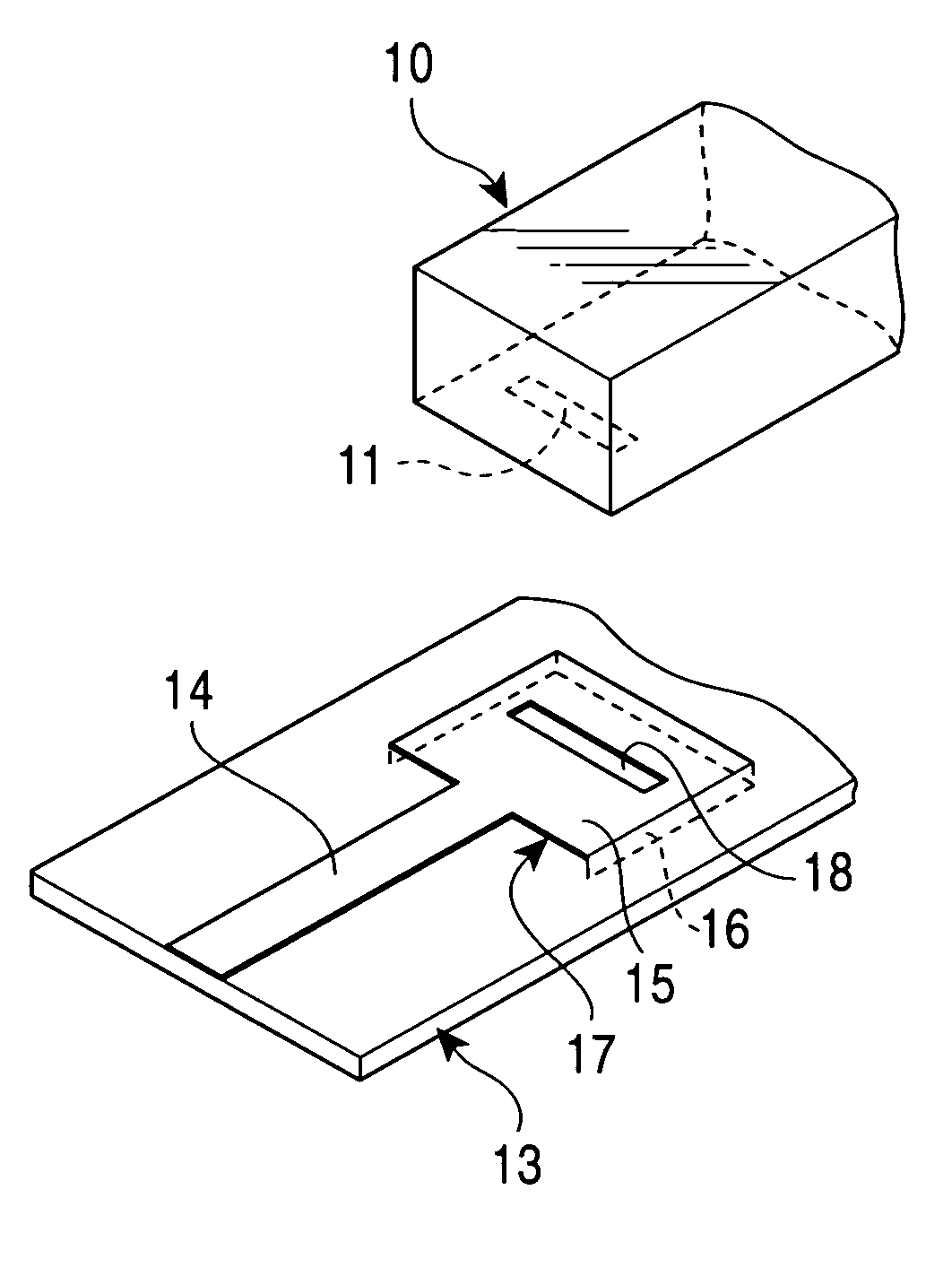
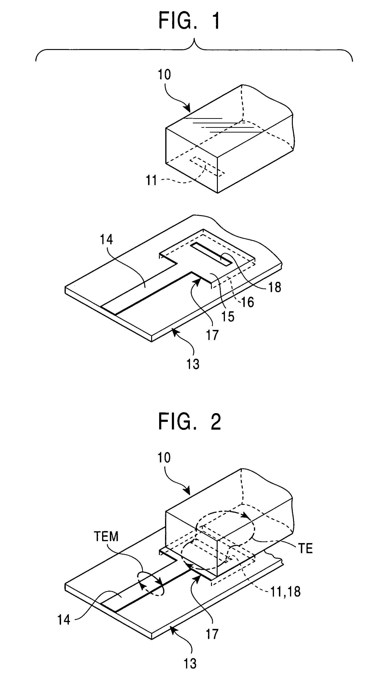
[0021]With reference to the drawings, various embodiments of the present invention will now be described. FIG. 1 is a perspective view showing a coupling structure between a dielectric waveguide resonator and a microstrip line according to one embodiment of the present invention. A printed circuit board 13 is provided with a microstrip line 14 and a mode conversion section 17 connected with the microstrip line 14. The mode conversion section 17 is formed as a rectangular cavity. The three sides of the cavity are surrounded by a conductive wall 16, and one side connected with the microstrip line 14 has no conductive wall. A conductive film 15 for the mode conversion section 17 is formed on the front surface of the printed circuit board 13. A part of the conductive film 15 is removed to form a slot 18 therein. A dielectric waveguide resonator 10 has a bottom surface formed with a conductive film. A part of the conductive film of the resonator 10 is also removed to form a slot 11 there...


PUM


Abstract

Disclosed is an input / output coupling structure for a dielectric waveguide resonator to be mounted on a printed circuit board, which comprises; a region defined in the printed circuit board and surrounded by a first conductive film formed on the front surface of the printed circuit board and connected to a microstrip line on the printed circuit board, a second conductive film formed on the back surface of the printed circuit board, and a conductive wall connecting the respective peripheries of the first and second conductive films; a first slot formed in the front surface of the region; and a second slot formed in a surface of the dielectric waveguide resonator which is disposed to be opposed to the region of the printed circuit board. The first and second slots are adapted to be disposed in opposed relation to one another. The coupling structure can achieve the connection between a dielectric waveguide resonator and a microstrip line without forming any input / output electrode on the resonator, to facilitate the application of the dielectric waveguide resonator to an electronic circuit even if it is intended to be used in millimetric-wave band.

Description

FIELD OF THE INVENTION[0001]The present invention relates to an input / output coupling structure between a microstrip line formed on a printed circuit board and a dielectric waveguide resonator, and more particularly to an input / output coupling structure for coupling between TEM mode in a microstrip line and TE mode in a dielectric waveguide resonator to perform the conversion between the modes.BACKGROUND OF THE INVENTION[0002][Patent Publication][0003]Japanese Patent Laid-Open Publication No. 2000-208806[0004][Non-Patent Publication][0005]Dominic Deslandes and Ke Wu, Integrated Microstrip and Rectangular Waveguide in Planar Form, IEEE Microwave and Wireless Component Letters, Vol. 11, No. 2, 2001.[0006]A dielectric waveguide resonator and a dielectric filter composed of a plurality of dielectric waveguide resonators coupled with each other constitute a circuit component having low-loss characteristics in microwave and millimetric-wave bands. A microstrip or coplanar line is widely u...

Claims


Application Information

Patent Timeline
Patent Type & Authority Patents(United States)
IPC IPC(8): H01P1/208H01P5/08H01P5/10H01P5/107
CPCH01P5/1022H01P5/107H01P1/2088
Inventor ITOH, KAZUHIROSANO, KAZUHISA
Owner MURATA MFG CO LTD
Why Eureka
Try Eureka