Light-emitting semiconductor device and method of fabrication

a technology of light-emitting semiconductors and manufacturing methods, which is applied in the manufacture of semiconductor/solid-state devices, semiconductor devices, electrical devices, etc., can solve the problems of increasing the manufacturing cost of sapphire devices, and additional difficulties in connection with sapphire base plates, etc., to achieve small lattice constraint difference, easy fabrication, and favorable performance characteristics

Inactive Publication Date: 2005-12-27
SANKEN ELECTRIC CO LTD
View PDF4 Cites 6 Cited by
  • Summary
  • Abstract
  • Description
  • Claims
  • Application Information

AI Technical Summary

Benefits of technology

[0026]The invention enables an easy and inexpensive fabrication of the light-emitting semiconductor device of the improved performance characteristics.

Problems solved by technology

The noted sapphire baseplate of the light-emitting devices has been a cause of trouble in such dicing of the wafers because of its extreme hardness.
Sapphire itself is expensive, moreover, adding much to the manufacturing costs of the light-emitting devices.
There have been additional difficulties in connection with the sapphire baseplate.
The results were a greater surface area of the semiconductor and a corresponding increase in the costs of the light-emitting devices.
A further inconvenience arose from the fact that current flows through the n-type semiconductor region not only vertically (normal to the plane of the sapphire baseplate) but horizontally (parallel to the sapphire baseplate plane).
A still further inconvenience concerns the etching-away of parts of the active layer and p-type semiconductor region in order to expose part of the n-type semiconductor region for connection to the cathode.
Offsetting these advantages, however, is the fact that SiC is even more expensive than sapphire.

Method used


Image

  • Light-emitting semiconductor device and method of fabrication
  • Light-emitting semiconductor device and method of fabrication

Examples


Embodiment Construction

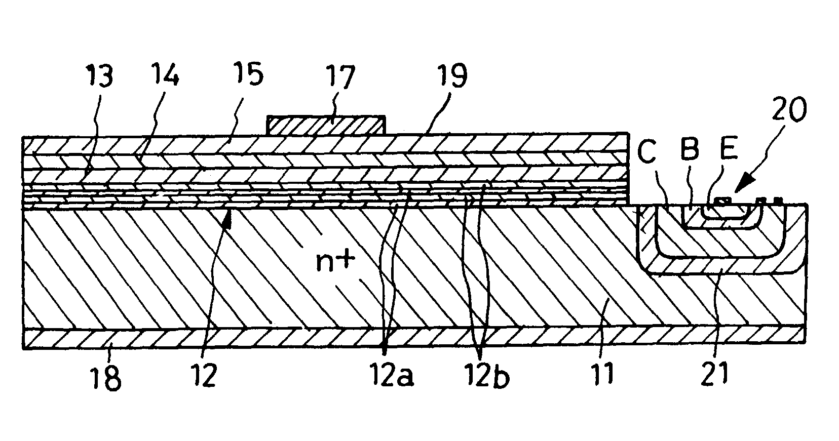
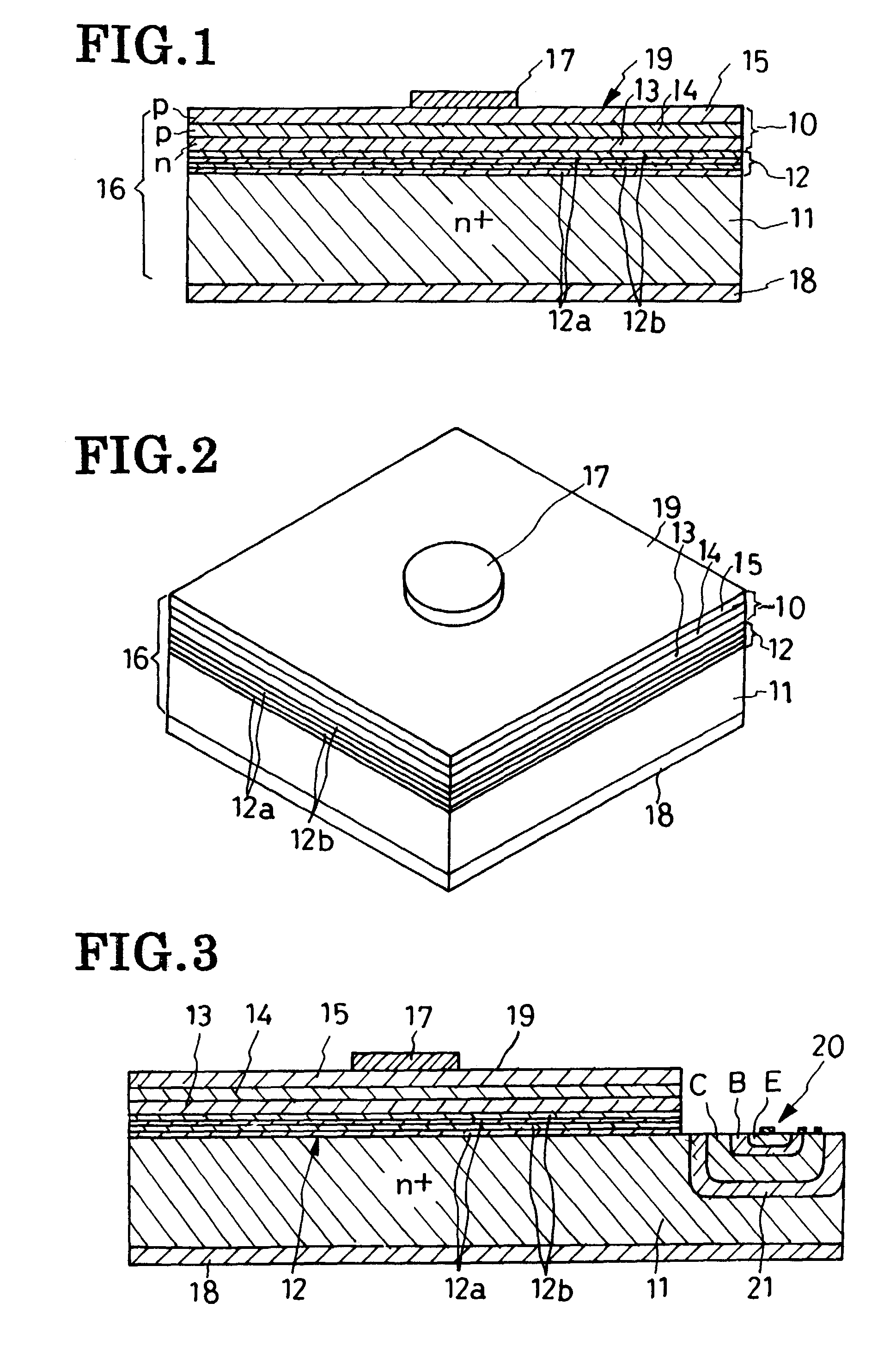
[0030]The light-emitting semiconductor device according to the invention will now be described in detail in terms of the blue-light-emitting GaN-based compound diode illustrated in FIGS. 1 and 2. The exemplified blue LED comprises a semiconductor region 10 composed of a plurality of GaN-based compound semiconductor layers for emission of light, a substrate or baseplate 11 of a silicon semiconductor having a crystal plane (111), and a buffer layer 12. The light-emitting semiconductor region 10 comprises an n-type semiconductor region 13 composed of GaN, a p-type light-emitting or active layer 14 composed of InGaN, and a p-type semiconductor region 15 composed of GaN.

[0031]The lamination of the light-emitting semiconductor region 10, the baseplate 11 and the buffer layer 12 constitutes a substrate or base body 16. An anode 17 is formed on one of the two opposite major surfaces, or on the top as seen in the attached drawings, of the base body 16, or on the semiconductor region 15, and ...


PUM


Abstract

A low-resistance silicon baseplate (11) has formed thereon a buffer layer 12 in the form of an alternating lamination of AlN sublayers (12a) and GaN sublayers (12b). On this buffer layer there are formed an n-type semiconductor region (13) of gallium nitride, an active layer (14) of gallium indium nitride, and a p-type semiconductor region (15) of gallium nitride, in that order. An anode (17) is formed on the p-type semiconductor region (15), and a cathode (18) on the baseplate (11).

Description

[0001]This is a continuation of application Ser. No. 09 / 958,822, filed Oct. 15, 2001 now abandoned which is a 371 of PCT / JP01 / 01161, filed Feb. 19, 2001.TECHNICAL FIELD[0002]This invention relates to a light-emitting semiconductor device composed primarily of gallium nitride (GaN)-based semiconductors, and to a method of making the same.BACKGROUND ART[0003]The compound semiconductors composed primarily of GaN have been used extensively for fabrication of light-emitting devices such as diodes that are capable of glowing in blue. Examples of such compound semiconductors include, in addition to GaN itself, gallium aluminum nitride (GaAlN), indium gallium nitride (InGaN), and indium gallium aluminum nitride (InGaAlN).[0004]A typical prior art light-emitting device of the kind under consideration comprises a baseplate of electrically insulating material such as sapphire, a buffer layer overlying the baseplate and composed for example of GaxAl1−xN, where x is greater than zero and not gre...

Claims


Application Information

Patent Timeline
Patent Type & Authority Patents(United States)
IPC IPC(8): H01L33/00H01L33/04H01L33/32
CPCH01L33/007H01L33/32H01L33/04
Inventor MOKU, TETSUJIOHTSUKA, KOHJIYANAGIHARA, MASATAKAKIKUCHI, MASAAKI
Owner SANKEN ELECTRIC CO LTD
Why Eureka
Try Eureka