Electrically-tunable optical devices

Active Publication Date: 2011-05-19
UNIV OF IOWA RES FOUND +1
View PDF3 Cites 5 Cited by
  • Summary
  • Abstract
  • Description
  • Claims
  • Application Information

AI Technical Summary

Benefits of technology

[0025]According to a sixth aspect of the present invention there is provided a method of forming a device, the method comprising: arranging two mutually immiscible conductive liquids to form an interface therebetween; localising a plurality of nanoparticles at the said interface, the said nanoparticles each having a first region formed of a semiconductor having a first bandgap, the first region being surrounded by a second region having a second bandgap, the second bandgap being larger than the first bandgap; a

Problems solved by technology

However, to date, control of the fundamental absorption edge of a quantum dot with an applied electric field, through the Stark effect [2], has been limited by the elect

Method used


Image

  • Electrically-tunable optical devices
  • Electrically-tunable optical devices
  • Electrically-tunable optical devices

Examples


Embodiment Construction

[0036]The present embodiments represent the best ways known to the applicants of putting the invention into practice. However, they are not the only ways in which this can be achieved.

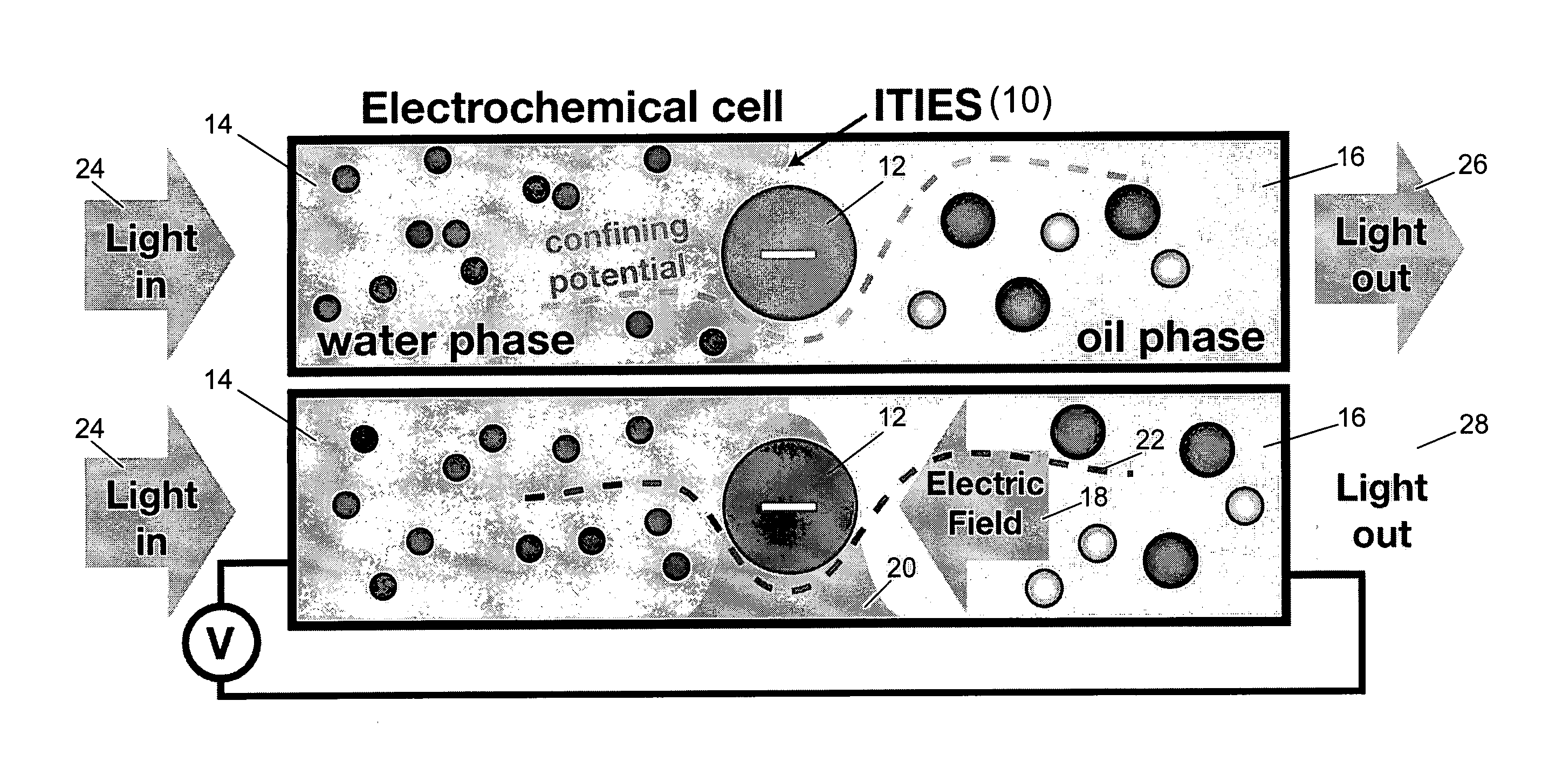
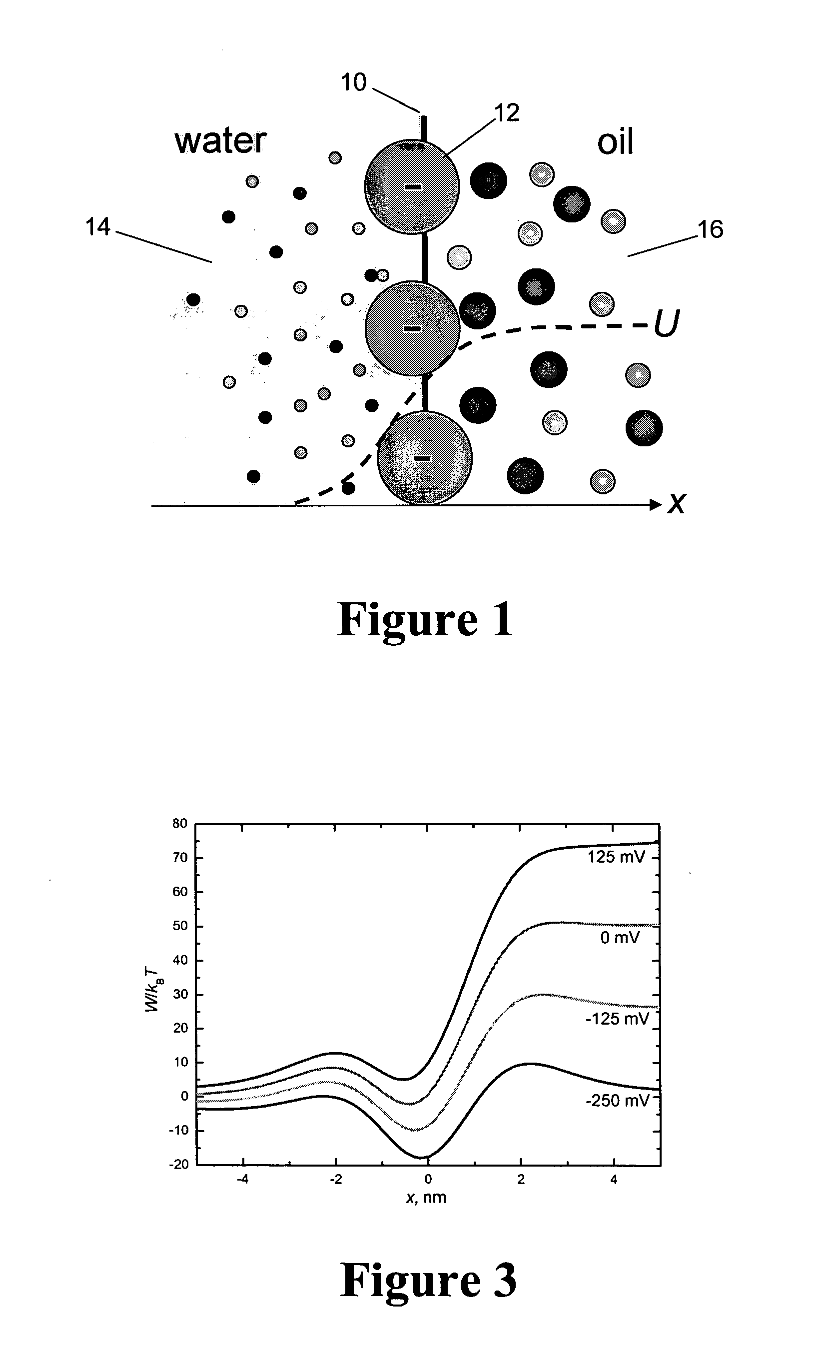
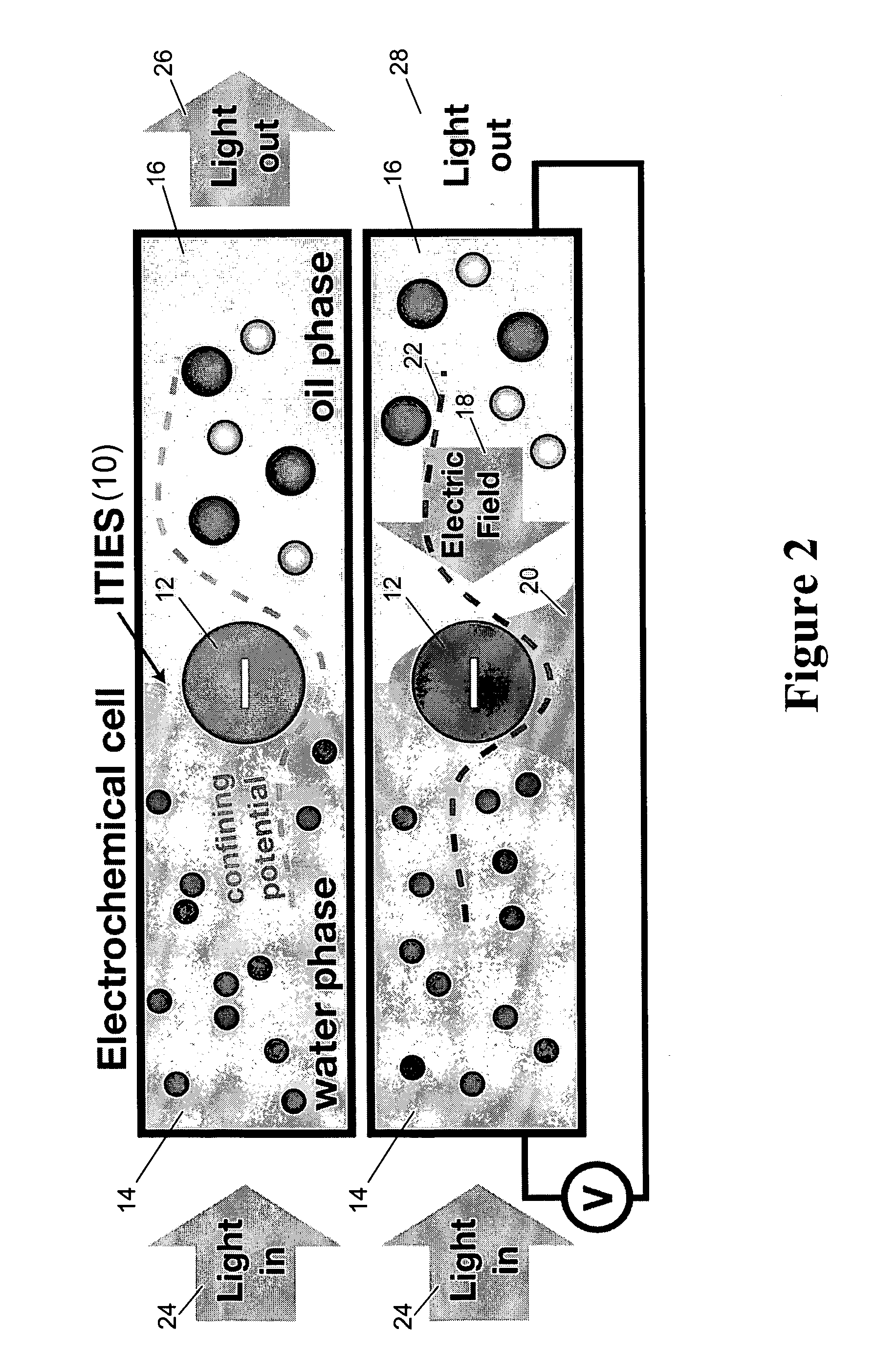
[0037]As mentioned above, control of the fundamental absorption edge of a quantum dot with an applied electric field, through the Stark effect[2], has to date been limited by the electrical breakdown of the material surrounding the dot. However, we have found that fields greatly in excess of those possible in semiconductor materials can be applied at an Interface of Two Immiscible Electrolytic Solutions (ITIES) in an electrochemical cell[3,4]. Furthermore, nanoparticles can be reversibly localised at this interface through the application of an electric field, whereupon they self-assemble in a two-dimensional layer. Semiconductor nanocrystals localized at an ITIES should have optical properties tunable across much of the visible spectrum, corresponding to at least 560-620 nm wavelength (green to red) f...


PUM


Abstract

A device comprising: two mutually immiscible conductive liquids arranged to form an interface therebetween; a plurality of nanoparticles localised at the said interface, the said nanoparticles each having a first region formed of a semiconductor having a first bandgap, the first region being surrounded by a second region having a second bandgap, the second bandgap being larger than the first bandgap; and means for applying an electric field to the said nanoparticles and thus, through the Stark effect, altering the optical absorption or emission characteristics of the nanoparticles.

Description

[0001]This invention relates to electrically-tunable optical devices. It is particularly suitable, but by no means limited, for use in optical filters and emitters. Such devices may operate within or outside the visible region of the electromagnetic spectrum.BACKGROUND TO THE INVENTION[0002]A quantum dot is a nanocrystalline material (also referred to herein as a nanoparticle) having a centre region typically of size 1-100 nm formed of a semiconductor having a first bandgap, the centre region being surrounded by a second region having a second bandgap, wherein the second bandgap is larger than the first. The second region may be, for example, a vacuum, or a second semiconductor. An example of a quantum dot uses cadmium selenide (CdSe) as the centre region and zinc sulphide (ZnS) as the surrounding second region, with ZnS having a larger bandgap than CdSe.[0003]Quantum dots have tunable electronic, optical and magnetic properties depending on the diameter of the nanocrystals from whi...

Claims


Application Information

Patent Timeline
IPC IPC(8): G02F1/23H01L33/58H01L31/0232H01L31/18B82Y20/00B82Y99/00
CPCG02B26/005B82Y20/00
Inventor FLATTE, MICHAEL EDWARDKORNYSHEV, ALEXEIURBAKH, MICHAEL
Owner UNIV OF IOWA RES FOUND
Why Eureka
Try Eureka