Method of forming FinFET gates without long etches

a technology of finfet gate and etches, which is applied in the field of dual-gated transistors, can solve the problems of large variation in current from the source to the drain, large input impedance of mosfet, and long vertical distance over which the spacer runs, so as to achieve accurate and reliable formation, accurate growth, and accurate control of height and thickness of the resulting finfet gate

Active Publication Date: 2006-01-24
GLOBALFOUNDRIES U S INC
View PDF5 Cites 24 Cited by
  • Summary
  • Abstract
  • Description
  • Claims
  • Application Information

AI Technical Summary

Benefits of technology

[0007]Accordingly, embodiments of the present invention relate to a method for forming a gate for a FinFET using a series of selectively deposited sidewalls along with other sacrificial layers to create a cavity in which a gate can be accurately and reliably formed. This technique avoids long directional etching steps to form critical dimensions of the gate that have contributed to the difficulty of forming FinFETs using conventional techniques. In particular, a sacrificial seed layer, from which sidewalls can be accurately grown, is first deposited over a silicon fin. Once the sacrificial seed layer is etched away, the sidewalls can be surrounded by another disposable layer. Etching away the sidewalls will result in cavities being formed that straddle the fin, and gate conductor material can then be formed within these cavities. Thus, the height and thickness of the resulting FinFET gate can be accurately controlled by avoiding a long direction etch down the entire height of the fin.

Problems solved by technology

A small change in gate voltage can cause a large variation in the current from the source to the drain.
This gives the MOSFET an extremely large input impedance.
While a taller fin provides a device with more performance, it also results in a longer vertical distance over which the spacer runs.

Method used


Image

  • Method of forming FinFET gates without long etches
  • Method of forming FinFET gates without long etches
  • Method of forming FinFET gates without long etches

Examples


Embodiment Construction

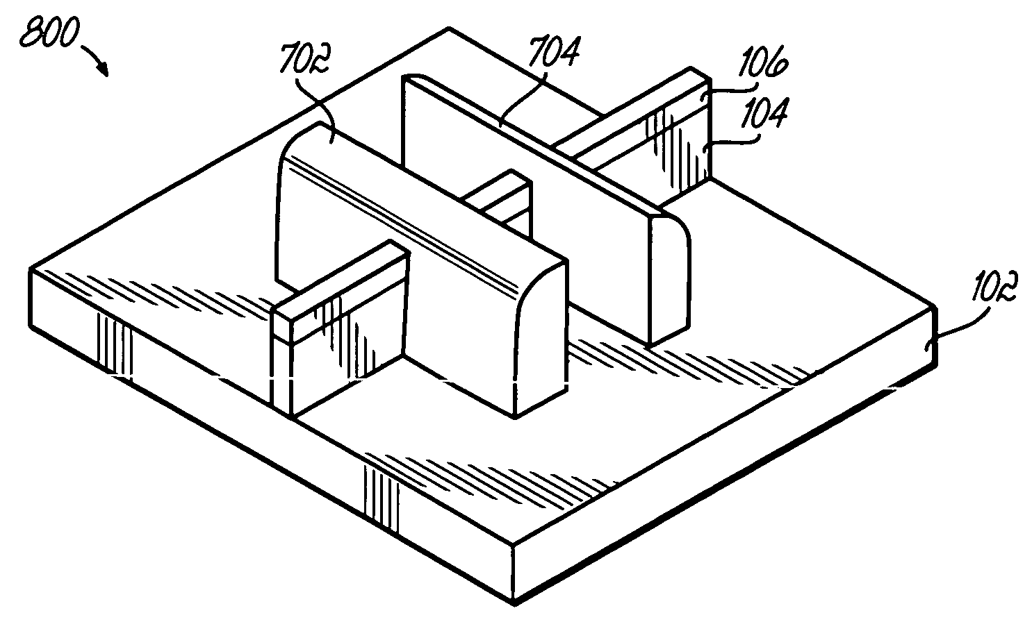
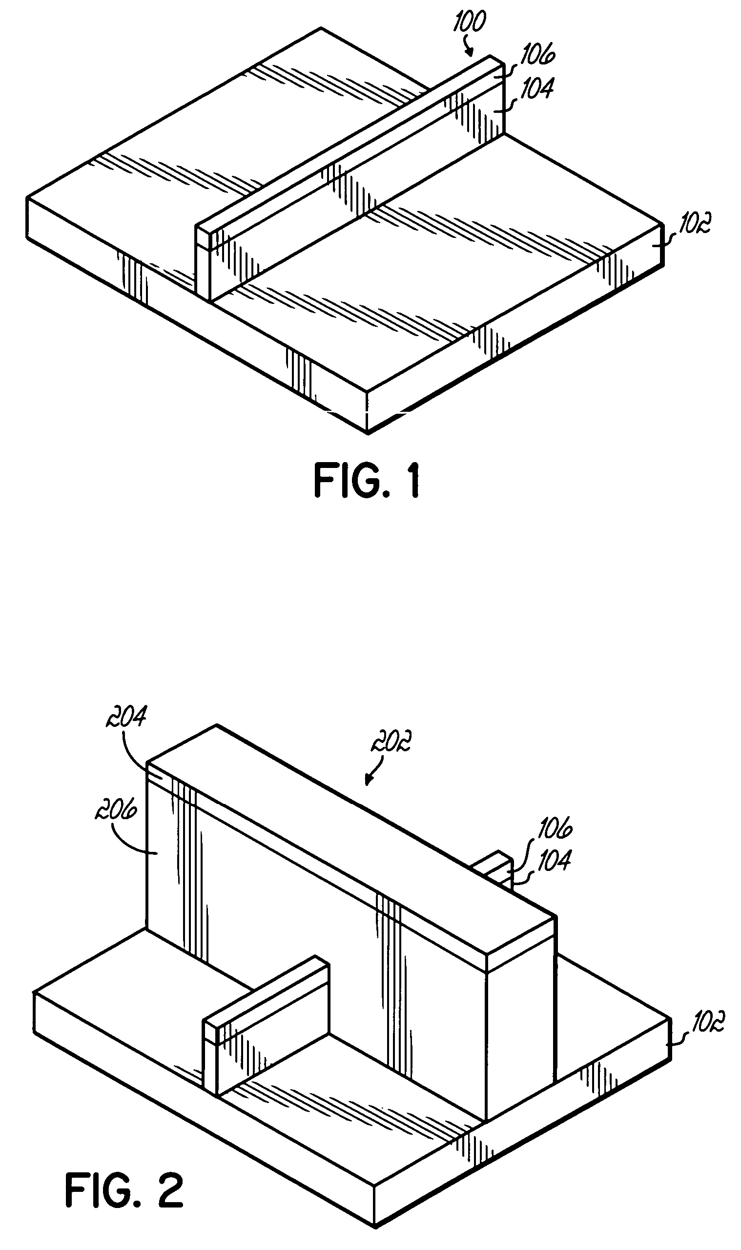
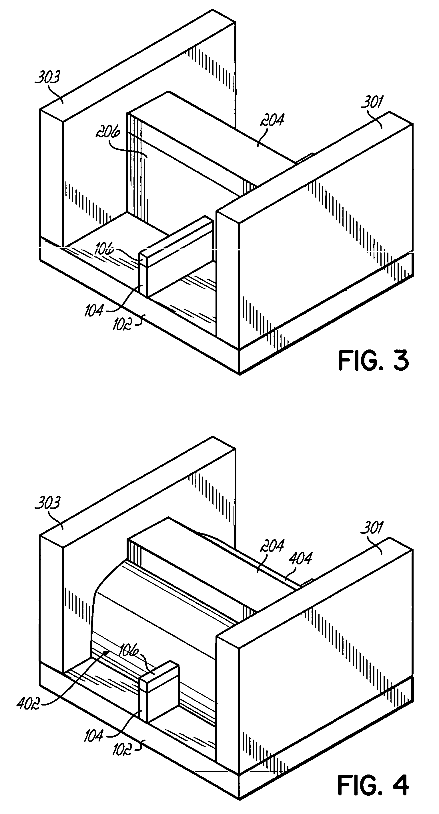
[0019]FIG. 1 depicts an initial structure in forming the FinFET. Using conventional photolithography techniques, a capped semiconductor fin 100, such as silicon, is formed on an insulating substrate 102. The capped semiconductor fin 100 includes protective nitride film 106 that is formed along the top of the semiconductor material 104. Next, referring to FIG. 2, a mandrel 202 is formed across the fin 100. Mandrel 202 is an organic material, the surface of which is then modified by exposure to a sililating agent such as hexamethyl-cyclotrisilazane or hexamethyl-disilazane. This exposure converts the surface of the mandrel 202 to a silicon containing organic polymer. This surface layer is subsequently oxidized in a dry oxygen containing plasma, such as RIE, downstream ozone, or such. As a result, the mandrel 202 is formed so as to facilitate selective oxide growth in liquid phase oxide deposition, but can be selectively stripped with respect to the growth oxide.

[0020]The mandrel mater...


PUM


Abstract

A method for forming a gate for a FinFET uses a series of selectively deposited sidewalls along with other sacrificial layers to create a cavity in which a gate can be accurately and reliably formed. This technique avoids long directional etching steps to form critical dimensions of the gate that have contributed to the difficulty of forming FinFETs using conventional techniques. In particular, a sacrificial seed layer, from which sidewalls can be accurately grown, is first deposited over a silicon fin. Once the sacrificial seed layer is etched away, the sidewalls can be surrounded by another disposable layer. Etching away the sidewalls will result in cavities being formed that straddle the fin, and gate conductor material can then be deposited within these cavities. Thus, the height and thickness of the resulting FinFET gate can be accurately controlled by avoiding a long direction etch down the entire height of the fin.

Description

FIELD OF THE INVENTION[0001]The present invention relates to dual-gated transistors and, more particularly, to FinFETs.BACKGROUND OF THE INVENTION[0002]A field-effect transistor (FET) is a type of transistor commonly used in Ultra Large Scale Integration (ULSI). In the FET, current flows along a semiconductor path called the channel. At one end of the channel, there is an electrode called the source. At the other end of the channel, there is an electrode called the drain. The physical dimensions of the channel are fixed, but its number of electrical carriers can be varied by the application of a voltage to a control electrode called the gate. The conductivity of the FET depends, at any given instant in time, on the number of electrical carriers of the channel. A small change in gate voltage can cause a large variation in the current from the source to the drain. This is how the FET amplifies signals. In one popular type of FET, known as a MOSFET, the channel can be either N-type or ...

Claims


Application Information

Patent Timeline
Patent Type & Authority Patents(United States)
IPC IPC(8): H01L21/336H01L21/00H01L29/786
CPCH01L29/66545H01L29/785H01L29/66795H01L29/7831
Inventor FURUKAWA, TOSHIHARUHAKEY, MARK CHARLESHOLMES, STEVEN JOHNHOFAK, DAVID VACLAVKOBURGER, III, CHARLES WILLIAMMITCHELL, PETER H.NESBIT, LARRY ALAN
Owner GLOBALFOUNDRIES U S INC
Why Eureka
Try Eureka