Method for designing an integrated circuit having multiple voltage domains

a technology of integrated circuits and voltage domains, applied in the field of integrated circuits, can solve the problems of labor-intensive process of designing such integrated circuits, adverse effects of voltage reduction on ac performance and noise immunity of integrated circuits,

Inactive Publication Date: 2006-02-14
INT BUSINESS MASCH CORP
View PDF8 Cites 80 Cited by
  • Summary
  • Abstract
  • Description
  • Claims
  • Application Information

AI Technical Summary

Problems solved by technology

However, these voltage reductions can have an adverse impact on the AC performance and noise immunity of integrated circuits.
However, even with modern design systems, designing such integrated circuits is a very labor-intensive process.

Method used


Image

  • Method for designing an integrated circuit having multiple voltage domains
  • Method for designing an integrated circuit having multiple voltage domains
  • Method for designing an integrated circuit having multiple voltage domains

Examples


Embodiment Construction

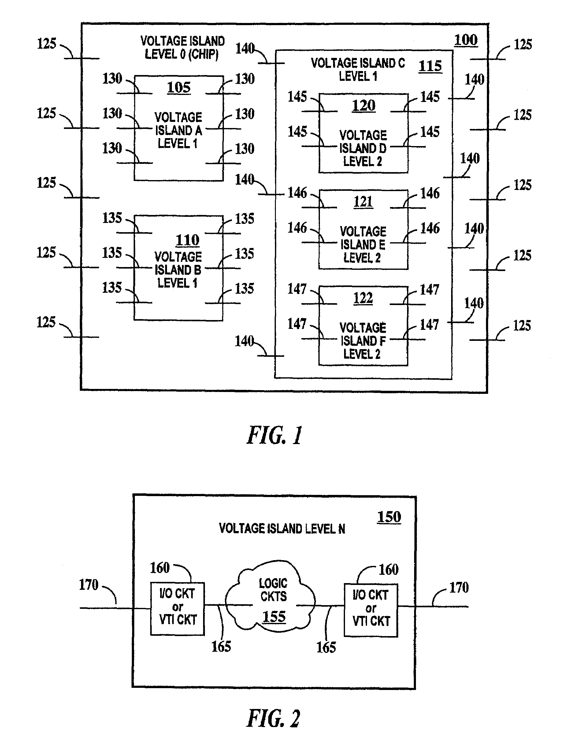
[0017]For the purposes of the present invention the terms voltage domain and voltage island are used interchangeably to denote the same entity, namely a bounded region of an IC chip having an internal power distribution network that is supplied from a power source external to that region. The term “designer” when used to describe the present invention refers to intervention by a human circuit designer. The terms “synthesizer,”“noise modeler,”“simulator,”“analyzer,” and “physical design tool” refer to software programs.

[0018]FIG. 1 is a diagram illustrating the partitioning of an exemplary IC 100 into voltage islands according to the present invention. In FIG. 1, IC chip 100 includes voltage island A 105, voltage island B 110 and voltage island C 115. IC chip 100 may be considered a voltage island itself. Voltage island C 115 further includes nested voltage island D 120, voltage island E 121 and voltage island F 122. As many levels of nesting of voltage islands as a particular IC des...


PUM


Abstract

A method for designing an integrated circuit having multiple voltage domains, including: (a) generating a logical integrated circuit design from information contained in a high-level design file, the high-level design file defining global connection declarations and voltage domain connection declarations; (b) synthesizing the logical integrated circuit design into a synthesized integrated circuit design based upon the logical integrated circuit design, information in a preferred components file and information in a voltage domain definition file; (c) generating a noise model from the synthesized integrated circuit design based on information in the voltage domain definition file and a design constraint file; and (d) simulating the noise model against constraints in the design constraint file and constraints in a circuit level profile file to determine if the synthesized integrated circuit design meets predetermined noise simulation targets.

Description

BACKGROUND OF INVENTION[0001]1. Field of the Invention[0002]The present invention relates to the field of integrated circuits; more specifically, it relates to a system and method for designing an integrated circuit having multiple voltage domains.[0003]2. Background of the Invention[0004]As integrated circuits have increased in complexity, voltages on power distribution networks have been reduced in order to reduce power consumption. However, these voltage reductions can have an adverse impact on the AC performance and noise immunity of integrated circuits. The use of voltage partitioning of an integrated circuit (IC) chip into voltage domains or islands allows some portions of an IC to operate at higher voltages for improved AC performance and noise immunity and other portions of the same IC to operate at a lower voltage for reduced power consumption.[0005]However, even with modern design systems, designing such integrated circuits is a very labor-intensive process. Therefore, the...

Claims


Application Information

Patent Timeline
Patent Type & Authority Patents(United States)
IPC IPC(8): G06F17/50G06G7/62
CPCG06F17/5045G06F30/30
Inventor IADANZA, JOSEPH A.SINGH, RAMINDERPALVENTRONE, SEBASTIAN T.WEMPLE, IVAN L.
Owner INT BUSINESS MASCH CORP
Why Eureka
Try Eureka