Pulse width modulator

a pulse width and modulator technology, applied in the direction of electric motor speed/torque regulation, dynamo-electric converter control, multiple dynamo-motor starters, etc., can solve the problem of unnecessary synchronization with paralleled circuits

Inactive Publication Date: 2006-02-28
BASKIN BRIAN L
View PDF9 Cites 16 Cited by
  • Summary
  • Abstract
  • Description
  • Claims
  • Application Information

AI Technical Summary

Benefits of technology

[0010]The present invention employs an output dependant clamping circuit. Rather than switching the clamping circuit synchronous with the positive switching circuit, the clamping circuit is energized when the output voltage drops below the negative supply voltage. A multitude of benefits is derived from this approach. First, the clamping circuit does not have to be aligned in order to prevent interference with the positive switching circuit. Second, synchronization with paralleled circuits is unnecessary as the design prevents the clamping circuit from interfering with other circuits. Finally, although the present clamping circuit is nearly as simple as a clamping diode, it provides a clamping efficiency comparable to a synchronous circuit.
[0011]In order to reduce emitted and conducted noise on both the power supply input and the output of the circuit, a unique method is utilized whereby the supply voltage is sampled, compared to a stable voltage, differentiated with respect to time, and multiplied by the low level switching voltage to increase rise and fall timing of the output signal. Unlike other methods, the present invention provides rise and fall times that are adaptive to the output load in order to minimize input and output noise of the system.

Problems solved by technology

Second, synchronization with paralleled circuits is unnecessary as the design prevents the clamping circuit from interfering with other circuits.

Method used


Image

  • Pulse width modulator
  • Pulse width modulator
  • Pulse width modulator

Examples


Embodiment Construction

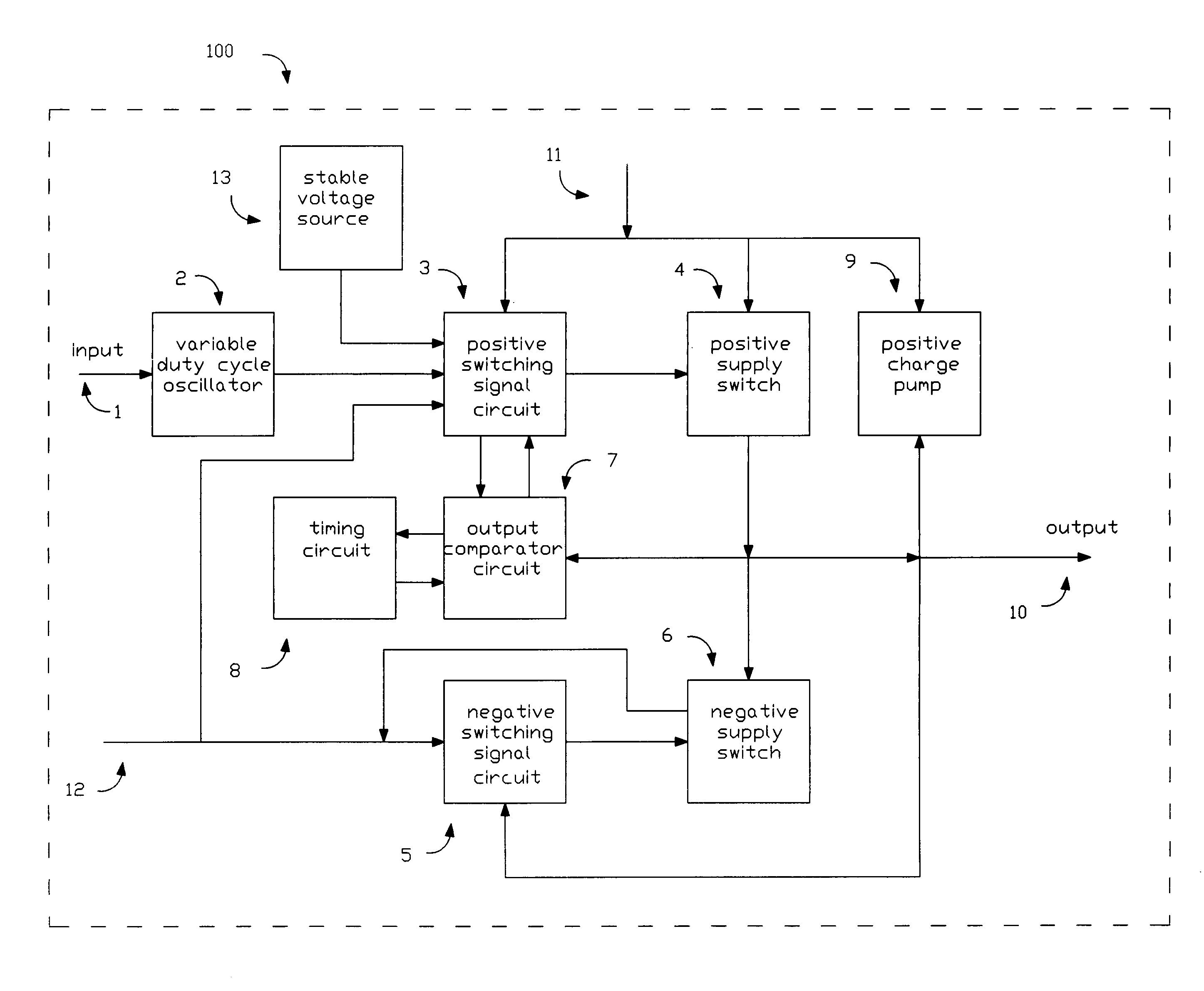
[0017]FIG. 1 shows a block diagram of the present embodiment of the invention. In FIG. 1 the pulse width modulator system (100) comprises a signal input port (1) a variable duty cycle oscillator (2) a positive switching signal circuit (3) a positive supply switch (4) a negative switching signal circuit (5) a negative supply switch (6) an output comparator circuit (7) a timing circuit (8), a positive charge pump (9) an output port (10), a positive voltage source input port (11) a negative voltage source input port (12), and a stable voltage source (13).

[0018]The variable duty cycle oscillator (2) provides an alternating current output signal, whereby the alternating current output signal duty cycle is a function of a received input voltage or current at the input signal port (1).

[0019]The positive switching signal circuit (3) receives the alternating current output signal, a first sample signal from the positive voltage source input port (11), a first sample signal from the negative ...


PUM


Abstract

The present invention encompasses a high efficiency pulse width modulator comprising: a variable duty cycle oscillator for receiving an input signal and providing a low level switching signal; a source voltage differentiation dependant positive switching signal circuit for receiving the low level switching signal, a stable reference signal, a sample of a positive supply voltage signal, and an error signal and the providing a positive supply switching signal and a reference signal; a positive supply switching circuit for receiving the positive supply switching signal and providing an output signal to an inductive load; an output voltage dependant negative supply switching signal circuit for receiving the output signal and a negative supply voltage signal and providing a negative supply switching signal; a negative supply switching circuit for receiving the negative supply switching signal and providing clamping of the inductive load to the negative supply, an output sourced charge pump for receiving the output signal and the positive supply voltage signal and providing a high voltage power supply; an output comparison circuit for receiving a sample of the output signal and a reference signal from the positive supply switching circuit, comparing the output signal to the reference signal and turning off the positive supply switching circuit when the output signal is lower than the reference signal; and a timing circuit for receiving an error signal from the comparison circuit and providing a feedback signal to the error circuit.

Description

BACKGROUND OF INVENTION[0001]1) Field of Invention[0002]This invention relates generally to voltage regulation devices and, more particularly to pulse width modulation.[0003]2) Description of Related Art[0004]Pulse width modulation has been employed for a number of years in order to attain high efficiency voltage regulation. There are, however, a plurality of drawbacks when utilizing pulse width modulation, in lieu of linear regulation in order to stabilize output voltage.[0005]Pulse width modulators generate both input and output noise not present in linear regulation. A pulse width modulator's efficiency is primarily due to the fact that the output voltage is either at substantially the input voltage or substantially at ground potential. The fast switching between the two states, necessary in order to achieve high efficiency regulation, also generates input noise as input current is switched to and from the load. Low switching times also contribute to emitted noise at the system o...

Claims


Application Information

Patent Timeline
Patent Type & Authority Patents(United States)
IPC IPC(8): H02P7/29
CPCH02P7/29
Inventor BASKIN, BRIAN L.
Owner BASKIN BRIAN L
Why Eureka
Try Eureka