Low stress and warpage laminate flip chip BGA package

a technology of laminate flip chip and package, applied in the direction of semiconductor devices, semiconductor/solid-state device details, electrical devices, etc., can solve the problems of package structure bowing, different temperatures, and exacerbated problems, and achieve the effect of improving industrial grade reliability, “soft” connection, and less bowing

Inactive Publication Date: 2006-03-07
ALTERA CORP
View PDF22 Cites 36 Cited by
  • Summary
  • Abstract
  • Description
  • Claims
  • Application Information

AI Technical Summary

Benefits of technology

[0007]To achieve the foregoing, the present invention provides a semiconductor die flip chip package with warpage control and improved industrial grade reliability. The present invention also provides fabrication methods for such packages. In general, the modulus of the adhesive, which is used to attach the heat spreader to the substrate, is selected to provide a relatively “soft” connection. The packages of the present invention include heat spreaders that are connected to the semiconductor die and packaging substrate with bonds that can withstand and redistribute the considerable bowing pressures caused by the CTE mismatches between the various package and die materials. The result is a semiconductor die flip chip package with less bowing and so improved co-planarity (in compliance with industry specifications) with the surface (e.g., PCB board) to which it is ultimately bound.

Problems solved by technology

A problem with such a semiconductor die flip chip package is that it is subject to different temperatures during the packaging process.
The high stress experienced by bonded materials during cooling may cause them to warp or crack and cause the package structure to bow.
In addition, this problem is exacerbated in the case of a relatively thick die processed from a larger diameter wafer, for example a 300 mm diameter wafer.
Low-K dielectric material layers in the low-K die are relatively brittle, rendering the low-K die susceptible to failure at even lower stress levels than conventional dice with FSG or USG dielectrics.

Method used


Image

  • Low stress and warpage laminate flip chip BGA package
  • Low stress and warpage laminate flip chip BGA package
  • Low stress and warpage laminate flip chip BGA package

Examples


example

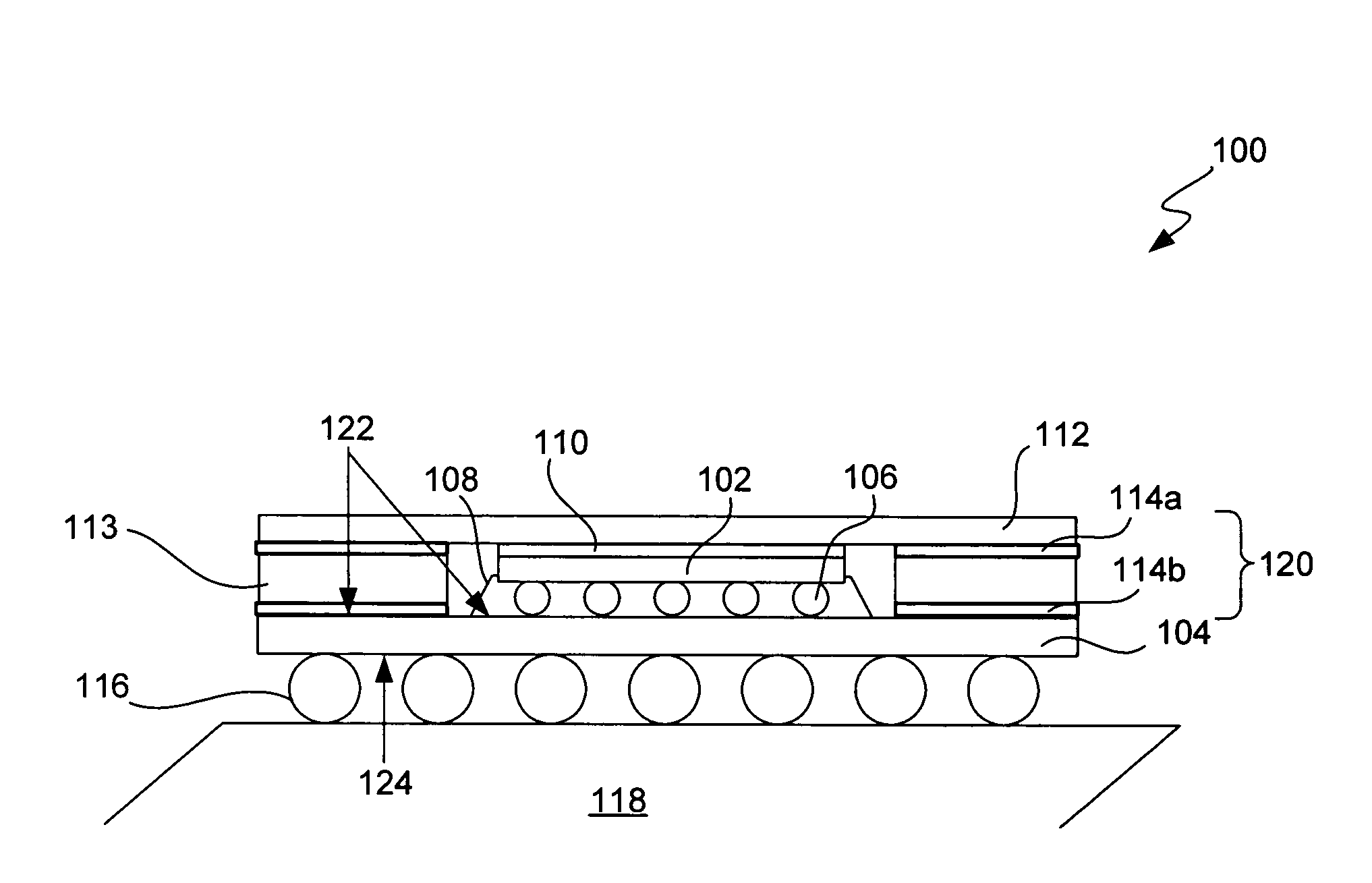
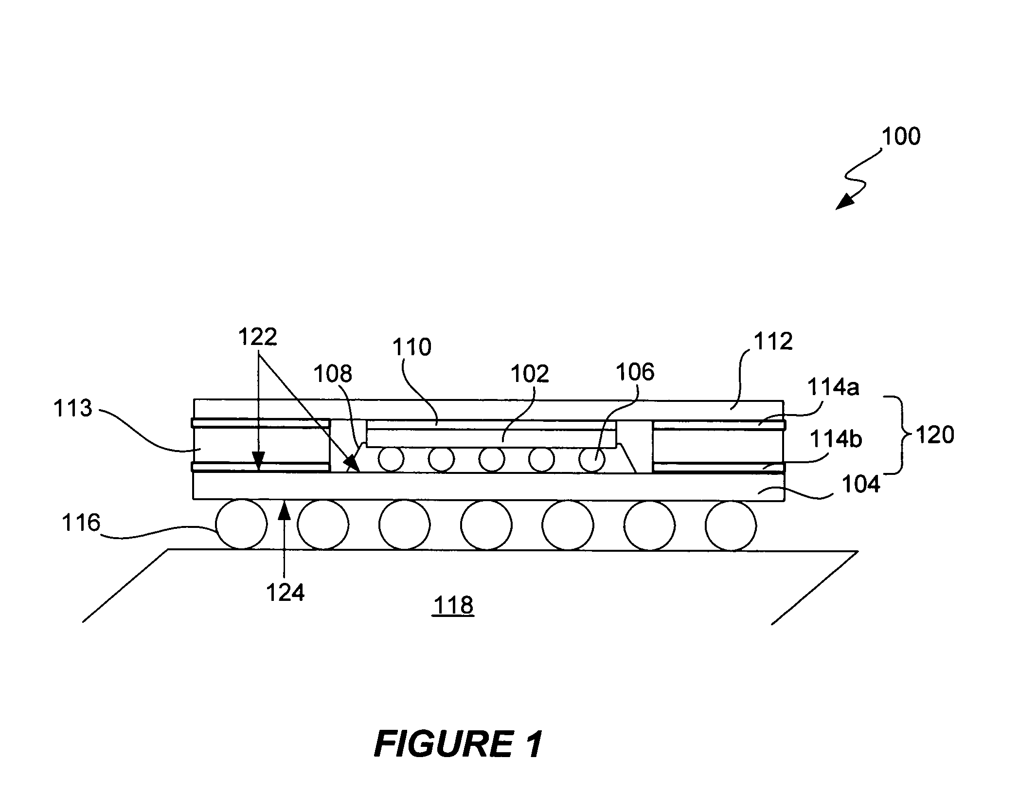
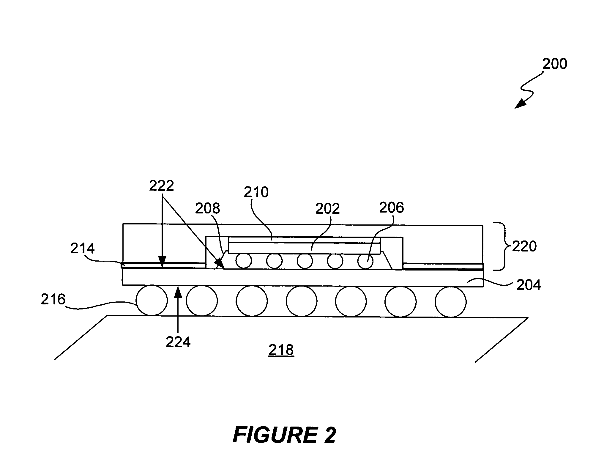
[0042]The following example provides modeling results for a semiconductor die flip chip package with warpage control in accordance with specific embodiments of the present invention. It should be understood the following is representative only, and that the invention is not limited by the detail set forth in this example.

[0043]A Stratix 1S60-F1020 die (e.g., 20 mm×22 mm die), available from Altera, Inc. of San Jose was selected along with a 33 mm×33 mm 6-layer build up organic substrate, available from Kyocera of Kyoto, Japan, in modeling a semiconductor die flip chip package in accordance to the present invention. The die had a CTE of about 2.6 ppm whereas the substrate had a CTE of about 17 ppm. The semiconductor die flip chip package was subjected to modeled warpage testing and to modeled reliability testing (e.g., industrial grade reliability test of thermal cycling condition B (−55° C. to 125° C.); JESD22-A104; Mil Std 1010) under different modeling arrangements to determine th...


PUM


Abstract

Provided are a semiconductor die flip chip package with warpage control and fabrication methods for such packages. The packages include heat spreaders that are attached to the die and packaging substrate. In general, the modulus of the adhesive, which is used to attach the heat spreader to the substrate, is selected to provide a relatively “soft” connection. The result is a package with less bowing and so improved co-planarity (e.g., in compliance with industry specifications) with the surface to which it is ultimately bound. Moreover, the die and package reliabilities are thereby enhanced.

Description

RELATED APPLICATIONS[0001]This application is a continuation-in-part of U.S. patent application Ser. No. 10 / 305,671, filed on Nov. 25, 2002, and entitled “FLIP CHIP PACKAGE WITH WARPAGE CONTROL”, incorporated herein by reference in its entirety for all purposes.BACKGROUND OF THE INVENTION[0002]This invention relates generally to semiconductor device package assembly, and in particular to semiconductor die flip chip package assembly. More specifically, the invention relates to an innovative material approach to lower stress and warpage in a laminate flip chip ball grid array (BGA).[0003]In semiconductor device package assembly, a semiconductor die (also referred to as an integrated circuit (IC) chip or “chip”) may be bonded directly to a packaging substrate. Such die is formed with bumps of solder affixed to its I / O bonding pads. During packaging, the die is “flipped” onto its front surface (e.g., active circuit surface) so that the solder bumps form electrical and mechanical connect...

Claims


Application Information

Patent Timeline
Patent Type & Authority Patents(United States)
IPC IPC(8): H01L23/48H01L23/52H01L29/40H01L21/44H01L21/48H01L21/50H01L23/367
CPCH01L21/50H01L23/3675H01L2924/10253H01L2924/01322H01L2924/01019H01L2224/16H01L2224/73253H01L2924/01012H01L2924/0102H01L2924/15311H01L2924/16152H01L2924/16195H01L2924/3511H01L2924/00H01L2924/351H01L2224/73204
Inventor LI, YUAN
Owner ALTERA CORP
Why Eureka
Try Eureka