Phase synchronization circuit
a phase synchronization and circuit technology, applied in the field of phase synchronization circuits, can solve the problems of circuits with large oscillation frequency variation, voltage controlled oscillation circuits, and inability to easily perform frequency acquisition to the desired condition, etc., and achieve the effect of extending the capture rang
- Summary
- Abstract
- Description
- Claims
- Application Information
AI Technical Summary
Benefits of technology
Problems solved by technology
Method used
Image
Examples
embodiment 1
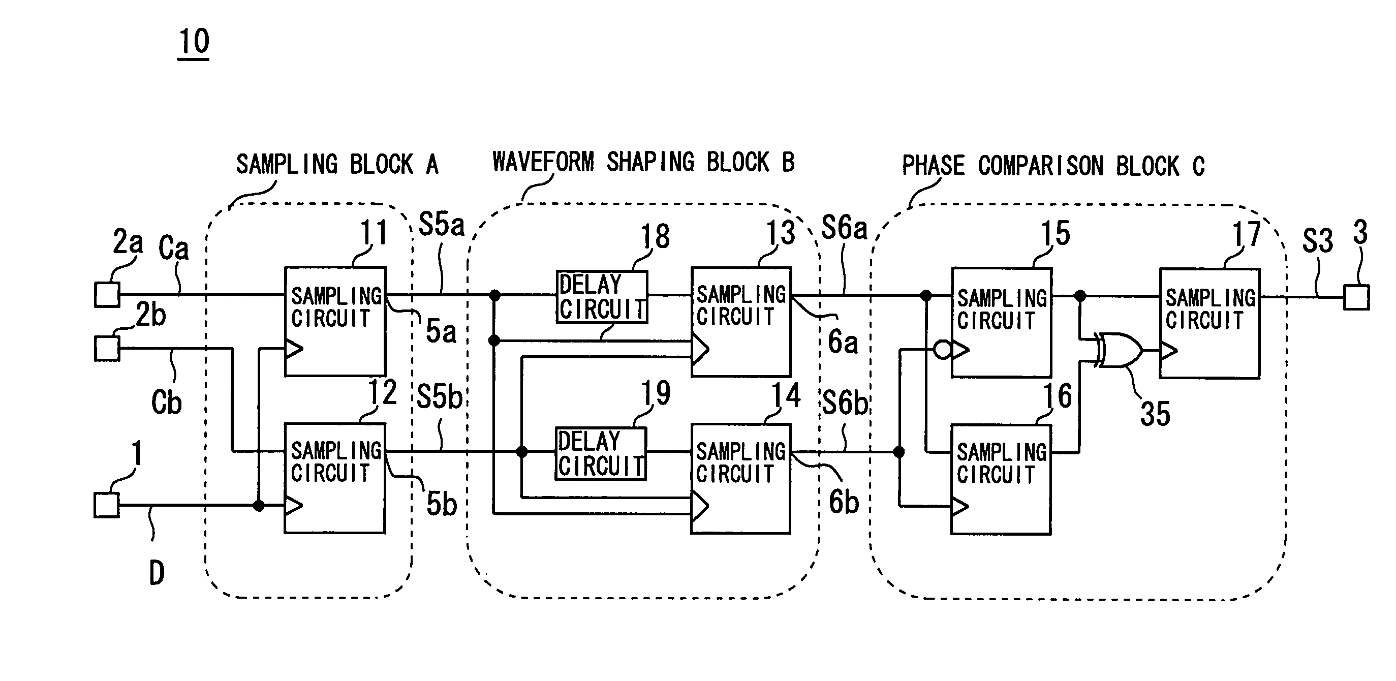
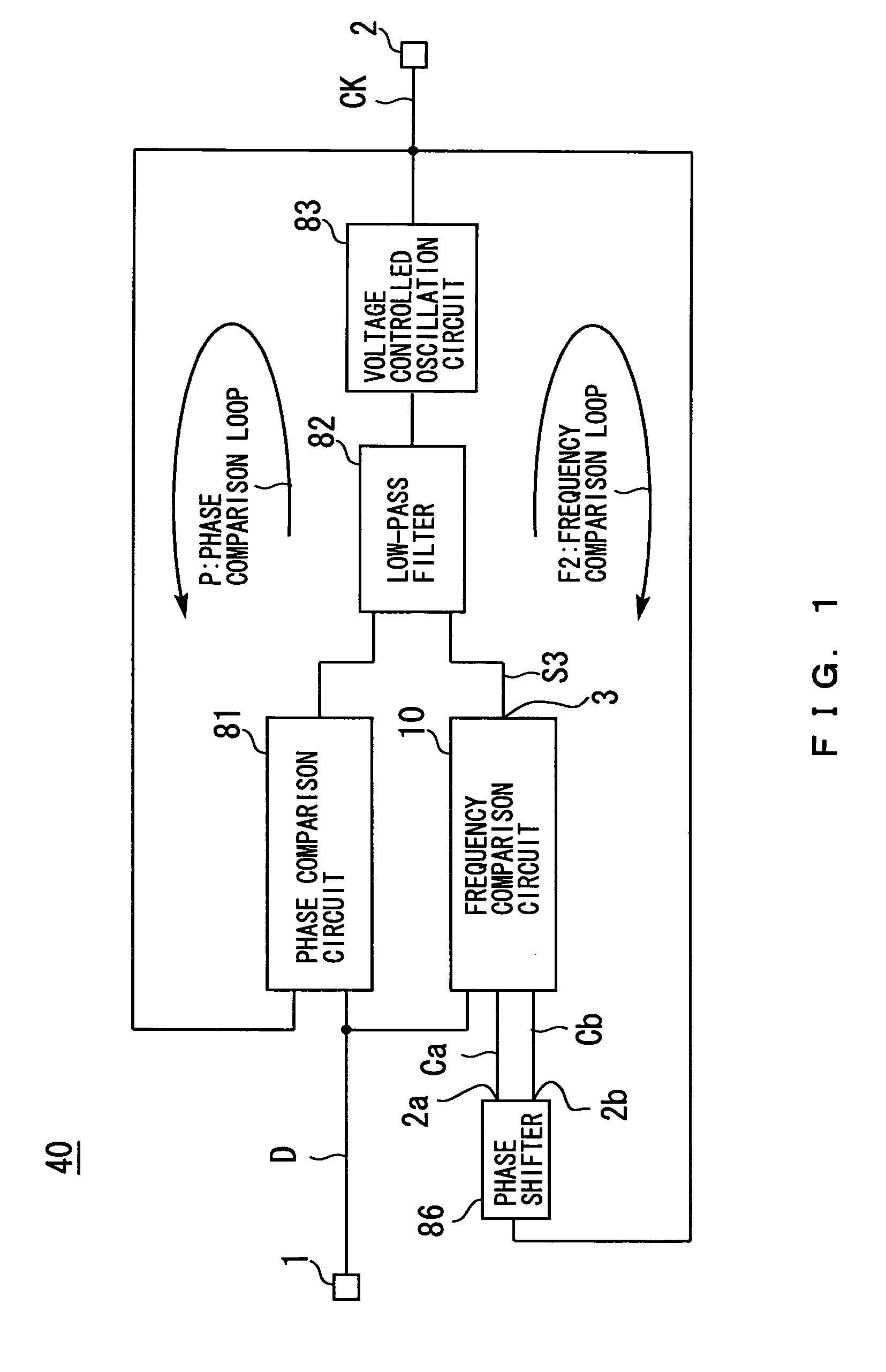
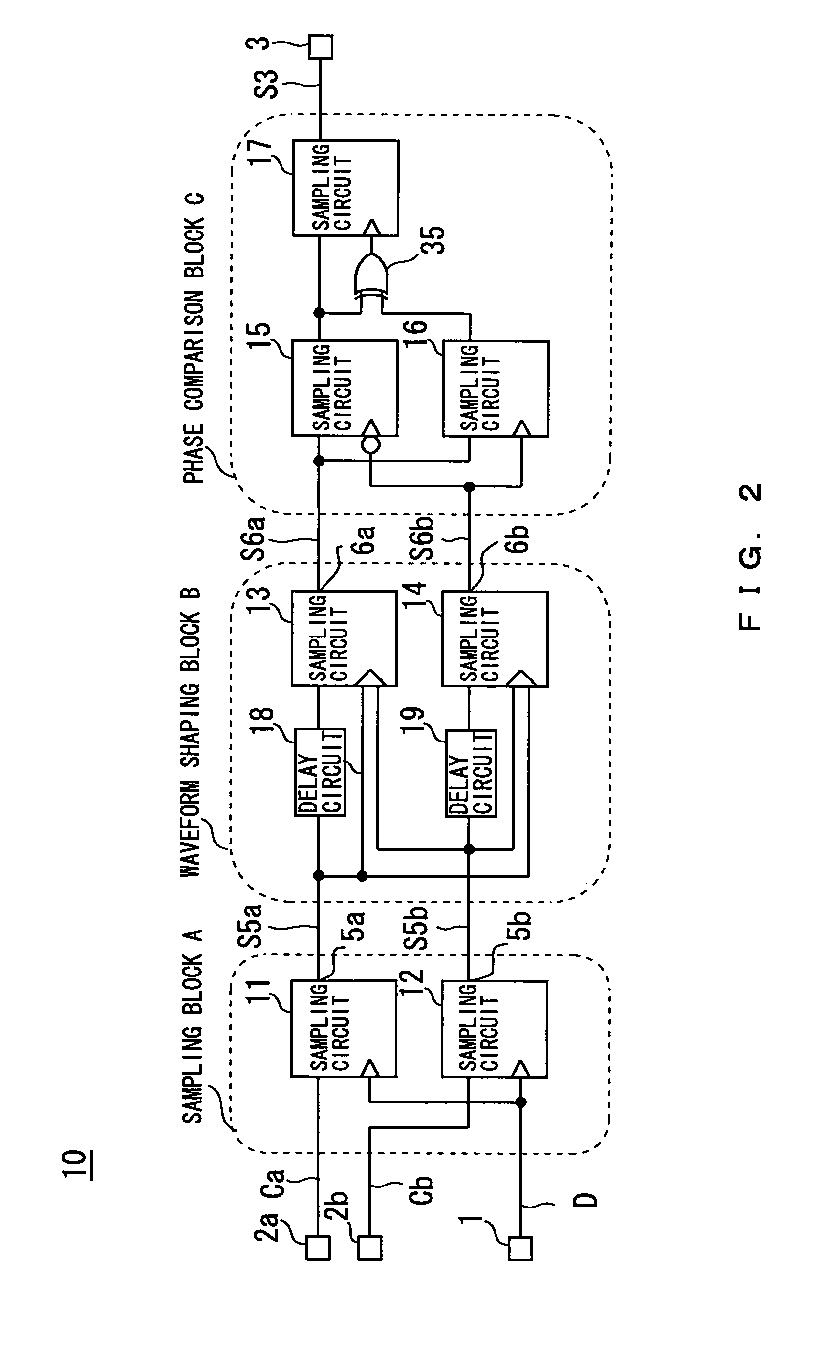
[0023]FIG. 1 is a block diagram of a phase sync circuit in Embodiment 1 of the present invention. In FIG. 1, symbol 40 denotes a phase sync circuit in accordance with the present invention, symbol 1 denotes an input terminal through which a data signal D in a random NRZ format is input; symbol 81 a phase comparison circuit which performs phase comparison between the data signal D input through the input terminal 1 and a signal CK output from a voltage controlled oscillation circuit 83 (described below); symbol 10 a frequency comparison circuit which performs frequency comparison between the data signal D input through the input terminal 1 and a signal Ca output from a terminal 2a of a phase shifter 86 (described below) or a signal Cb output from a terminal 2b of the phase shifter 86, and which produces an output through a terminal 3; symbol 82 a low-pass filter to which both a phase comparison result obtained by the phase comparison circuit 81 and a frequency comparison result obtai...
embodiment 2
[0057]Embodiment 1 has been described with respect to the operation of the frequency comparison circuit 20 in the phase sync circuit 40 of the present invention. There are some variations of the circuit configuration for realization this operation typified by one in Embodiment 2 described below.
[0058]FIG. 10 shows a circuit forming a sampling block A2 in Embodiment 2 of the present invention. Portions indicated in FIG. 10 by the same symbols as those in FIG. 3 have the same functions. No description will be made of the portions having the same functions. In FIG. 10, symbol 60 denotes another sampling block A2 corresponding to the implementation of the sampling block A, and symbols 61 and 62 denote D flip flop circuits. The sampling block A2 (60) is used instead of the sampling block A in the frequency comparison circuit 20 shown in FIG. 3 to make the minimum value of the pulse width in the signals S5a and S5b appearing at the terminals 5a and 5b about twice the pulse width at the sa...
embodiment 3
[0060]As the circuit for implementation of the phase comparison block C in the frequency comparison circuit 20 described above in the description of Embodiment 1, a different circuit such as one in Embodiment 3 may be implemented.
[0061]FIG. 11 shows the circuit in a phase comparison block C2 in Embodiment 3 of the present invention. Portions indicated in FIG. 11 by the same symbols as those in FIG. 3 have the same functions. No description will be made of the portions having the same functions. In FIG. 11, symbol 70 denotes another phase comparison block C2 corresponding to the implementation of the phase comparison block C; symbols 71 to 75 denote D flip flop circuits; symbols 63 to 68 denote AND circuits; symbol 69 denotes an OR circuit; and symbols 94 to 99 denote NOT circuits. The phase comparison block C2 (70) is used instead of the phase comparison block C in the frequency comparison circuit 20 shown in FIG. 3 to improve the accuracy with which verification is performed on the...
PUM
 Abstract
Description
Claims
Application Information


