Amplifying solid-state imaging device, and method for driving the same
a solid-state imaging and amplifier technology, applied in the field of amplifier solid-state imaging devices and a driving method, can solve the problems of horizontal noise appearing on the screen and degrading the resultant image quality, and achieve the effect of eliminating horizontal noise and eliminating horizontal noise from the screen
- Summary
- Abstract
- Description
- Claims
- Application Information
AI Technical Summary
Benefits of technology
Problems solved by technology
Method used
Image

Examples
first embodiment
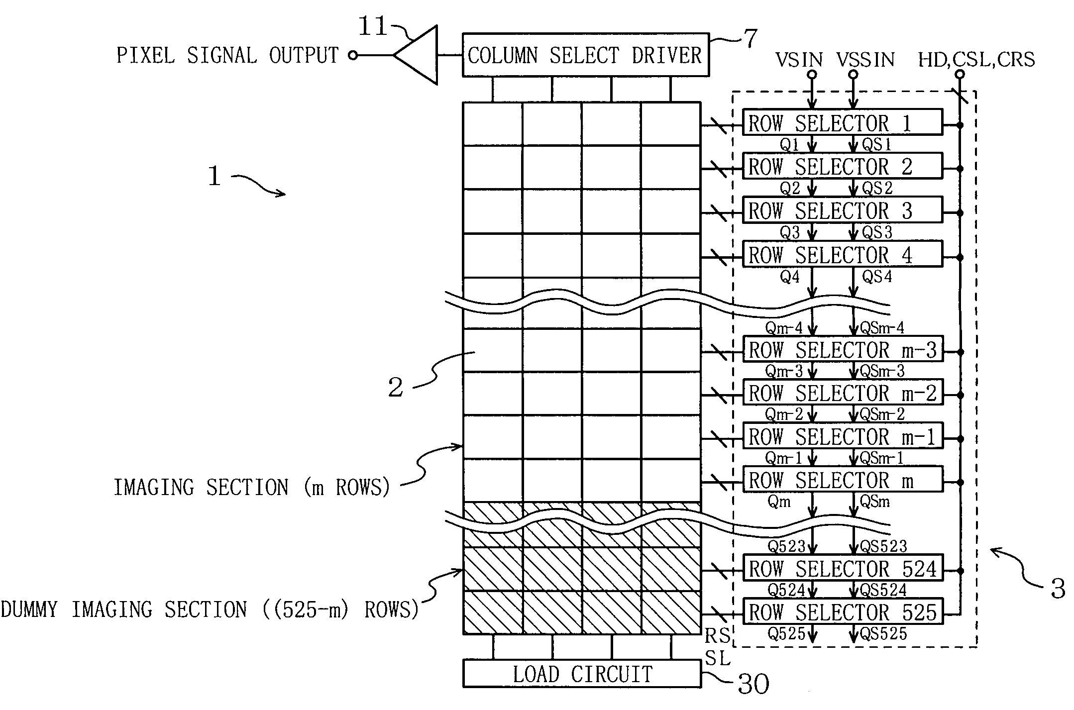
[0036]Next, the feature of the amplifying solid-state imaging device 1 will be described with reference to FIG. 3. As shown in FIG. 3, the device 1 additionally includes at least one dummy pixel row, which is provided separately from the number m of ordinary pixel rows. The number m of pixel rows are located within an effective pixel area and make up an imaging section. On the other hand, the at least one dummy pixel row is located out of the effective pixel area and makes up a dummy imaging section. According to this embodiment, the number of the dummy pixel row(s) is obtained by subtracting m from the number of horizontal sync signals included in one frame interval. In this specification, the number of the horizontal sync signals per frame interval will be called an “HD number”. In this exemplary embodiment, since m is 480 and the HD number is 525 (in compliance with the NTSC standard), the number of the dummy pixel row(s) (=HD number−m) is 45.
[0037]Each of the pixels belonging t...
second embodiment
[0078] even if the number of horizontal sync signals included in one frame interval has been changed, the device 60 still can operate normally.
[0079]FIG. 18 illustrates a configuration for an amplifying solid-state imaging device 70 according to a third embodiment of the present invention. The device 70 is different from the device 60 of the second embodiment in the construction of the dummy row selector. The dummy row selector B according to the third embodiment may have a configuration shown in FIG. 19. Responsive to the output Qm of the mth row selector, the dummy row selector B starts to output the control signals SLdummy and RSdummy in synchronism with the horizontal sync signal HD. Thereafter, the dummy row selector B continuously outputs the control signals SLdummy and RSdummy in synchronism with the horizontal sync signal HD until the selector B receives the start pulse signal VSIN or until resetting for the electronic shuttering operation on the mth row ends.
third embodiment
[0080]FIG. 20 is a timing diagram illustrating control signals supplied from the row selectors in the row select encoder 3 and the dummy row selector B within the amplifying solid-state imaging device 70 according to the As shown in FIG. 20, after the readout operation has been performed on the mth row and until resetting for the electronic shuttering operation on the mth row ends, the row select signal SLdummy and the reset signal RSdummy are repeatedly output in synchronism with the horizontal sync signal HD. Thus, after the readout operation has been performed on all the rows within the ordinary imaging section and before resetting for the electronic shuttering operation has been performed on all the rows within the ordinary imaging section, the readout operation is repeatedly performed on the dummy row, not on the ordinary imaging section. As a result, resetting for the electronic shuttering operation is performed under the same condition on all the rows within the ordinary ima...
PUM
 Abstract
Description
Claims
Application Information
 - R&D
- Intellectual Property
- Life Sciences
- Materials
- Tech Scout
- Unparalleled Data Quality
- Higher Quality Content
- 60% Fewer Hallucinations
Browse by: Latest US Patents, China's latest patents, Technical Efficacy Thesaurus, Application Domain, Technology Topic, Popular Technical Reports.
© 2025 PatSnap. All rights reserved.Legal|Privacy policy|Modern Slavery Act Transparency Statement|Sitemap|About US| Contact US: help@patsnap.com