Non-volatile memory and control with improved partial page program capability

a technology of partial page program and non-volatile memory, applied in static storage, digital storage, instruments, etc., can solve the problems of increasing the charge of the charge storage element, the difficulty of performing both these functions, and the programming of the charge storage memory devi

Active Publication Date: 2006-06-06
SANDISK TECH LLC
View PDF28 Cites 175 Cited by
  • Summary
  • Abstract
  • Description
  • Claims
  • Application Information

AI Technical Summary

Benefits of technology

[0057]According to another aspect of the invention, flag cells for storing flag data may be used to indicate the boundary of host or user data, such as the end of host or use data, so that the partial program problem does not lead to erroneous results. In one embodiment, the elements are grouped into a plurality of sectors or groups, each group including at least one corresponding flag charge storage cell for storing flag data that indicate whether elements of such group has been programmed or not in the second pass when there is insufficient host data. At least two of the plurality of groups are controlled by a common word line. When there is sufficient host data to program at least one but not all of the at least two groups during the second pass, flag data is stored in at least one of the flag charge storage cell(s) in the at least two groups, or the flag data stored in such flag cell(s) is altered, to indicate a boundary of the host data.

Problems solved by technology

It is often difficult to perform both of these functions in an optimum manner with a single voltage.
Programming of charge storage memory devices can only result in adding more charge to its charge storage elements.
The problem occurs most pronouncedly between two sets of adjacent cells that have been programmed at different times. One set of cells is programmed to add a level of charge to the floating gates that corresponds to one set of data.
In other words, when a host is transferring user data to the memory array, towards the end of the data transfer, there may be insufficient user data to completely program all of the memory cells in the page.
Thus, if each row of 2048 memory cells is divided into two interleaved pages, such as odd and even pages, so that each page contains 1024 bytes, there may only be adequate or sufficient data to fill the even or odd first page and one but not both of the sectors of the even or odd second page.
However, where a different code scheme is used, such as those shown in FIGS. 5A, 5B and 5C described above, this can become a problem as illustrated below.
From FIG. 5C, it is observed that the state “10” storage level is the highest level C. Since existing programming techniques do not permit the threshold voltage of storage level of individual memory cells to be reduced apart from the block erase operation, it would not be feasible to reprogram such memory cells from the states “10” to the state “00” if the code scheme of FIGS. 5A–5C is used, which results in the cells being programmed to the wrong state.

Method used


Image

  • Non-volatile memory and control with improved partial page program capability
  • Non-volatile memory and control with improved partial page program capability
  • Non-volatile memory and control with improved partial page program capability

Examples


Embodiment Construction

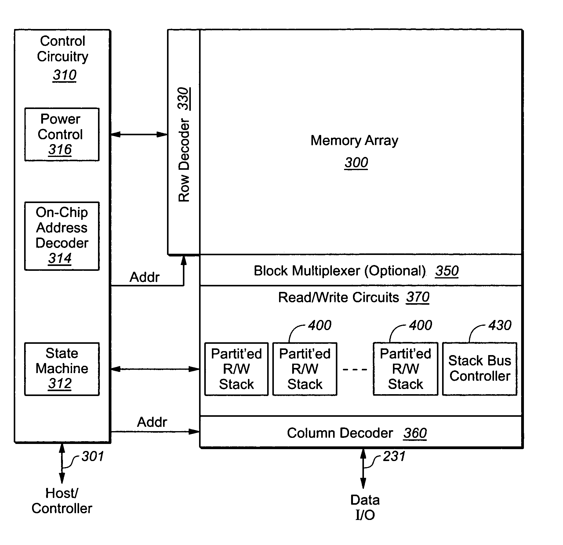
Example Non-Volatile Memory System:

[0073]FIG. 7 is a schematic block diagram of an individual read / write module 200 partitioned into a core portion 210 and a common portion 220, according to a preferred embodiment of the present invention. The core portion 210 comprises a sense amplifier 212 that determines whether a conduction current in a connected bit line 211 is above or below a predetermined threshold level. As described above, the connected bit line 211 enables access to the drain of an addressed memory cell in an array.

[0074]In one embodiment, the core portion 210 also includes a bit line latch 214. The bit line latch is used to set a voltage condition on the connected bit line 211. In one implementation, a predetermined state latched in the bit line latch will result in the connected bit line 211 being pulled to a state designating program inhibit (e.g., Vdd). This feature is used for program inhibition as will be described below.

[0075]The common portion 220 comprises a proc...


PUM


Abstract

In a non-volatile memory programming scheme where the memory cells are programmed in two or more sequential programming passes, when there is insufficient host data to program at least some of the memory cells during the second pass, some of the memory cells may be programmed to the wrong threshold voltage. This can be prevented by modifying the programming scheme so that this does not occur. In one implementation, this is accomplished by choosing a code scheme, which does not cause the memory cells to be programmed to the wrong threshold voltage during the second programming pass, or by programming the memory cells in accordance with substitute data that would not cause the cells to be programmed to an erroneous state.

Description

BACKGROUND OF THE INVENTION[0001]This invention relates generally to non-volatile semiconductor memories such as electrically erasable programmable read-only memory (EEPROM) and flash EEPROM, and specifically ones with improved partial page program capability.[0002]Solid-state memory capable of nonvolatile storage of charge, particularly in the form of EEPROM and flash EEPROM packaged as a small form factor card, has recently become the storage of choice in a variety of mobile and handheld devices, notably information appliances and consumer electronics products. Flash memory, both embedded and in the form of a removable card is ideally suited in the mobile and handheld environment because of its small size, low power consumption, high speed and high reliability features.[0003]EEPROM utilizes a floating (unconnected) conductive gate, in a field effect transistor structure, positioned over a channel region in a semiconductor substrate, between source and drain regions. A control gate...

Claims


Application Information

Patent Timeline
Patent Type & Authority Patents(United States)
IPC IPC(8): G11C16/04G11C11/56G11C16/10
CPCG11C11/5628G11C11/5642G11C16/10G11C2211/5646G11C16/0483H10B20/20
Inventor LI, YANFONG, YUPIN KAWINGMIWA, TORU
Owner SANDISK TECH LLC
Why Eureka
Try Eureka