Flash memory with sequential programming

a flash memory and sequential programming technology, applied in the field of flash memory devices, can solve the problems of power noise, program current may create power noise, and the upper limit of the power supply output current of the tester unit for testing memory devices

Active Publication Date: 2009-04-28
ELITE SEMICON MEMORY TECH INC
View PDF12 Cites 5 Cited by
  • Summary
  • Abstract
  • Description
  • Claims
  • Application Information

AI Technical Summary

Problems solved by technology

This large programming current may create power noise.
Therefore, there is a voltage drop due to the large current flowing across these connection lines leading to power noise.
Further, tester units for testing memory devices have upper limits for power supply output current.
Therefore, high current consumption by chips limits the number of chips that can be tested at one time by the tester.
This bit line leakage current can cause the regulated voltage to drop below the voltage level necessary for programming.

Method used


Image

  • Flash memory with sequential programming
  • Flash memory with sequential programming
  • Flash memory with sequential programming

Examples


Embodiment Construction

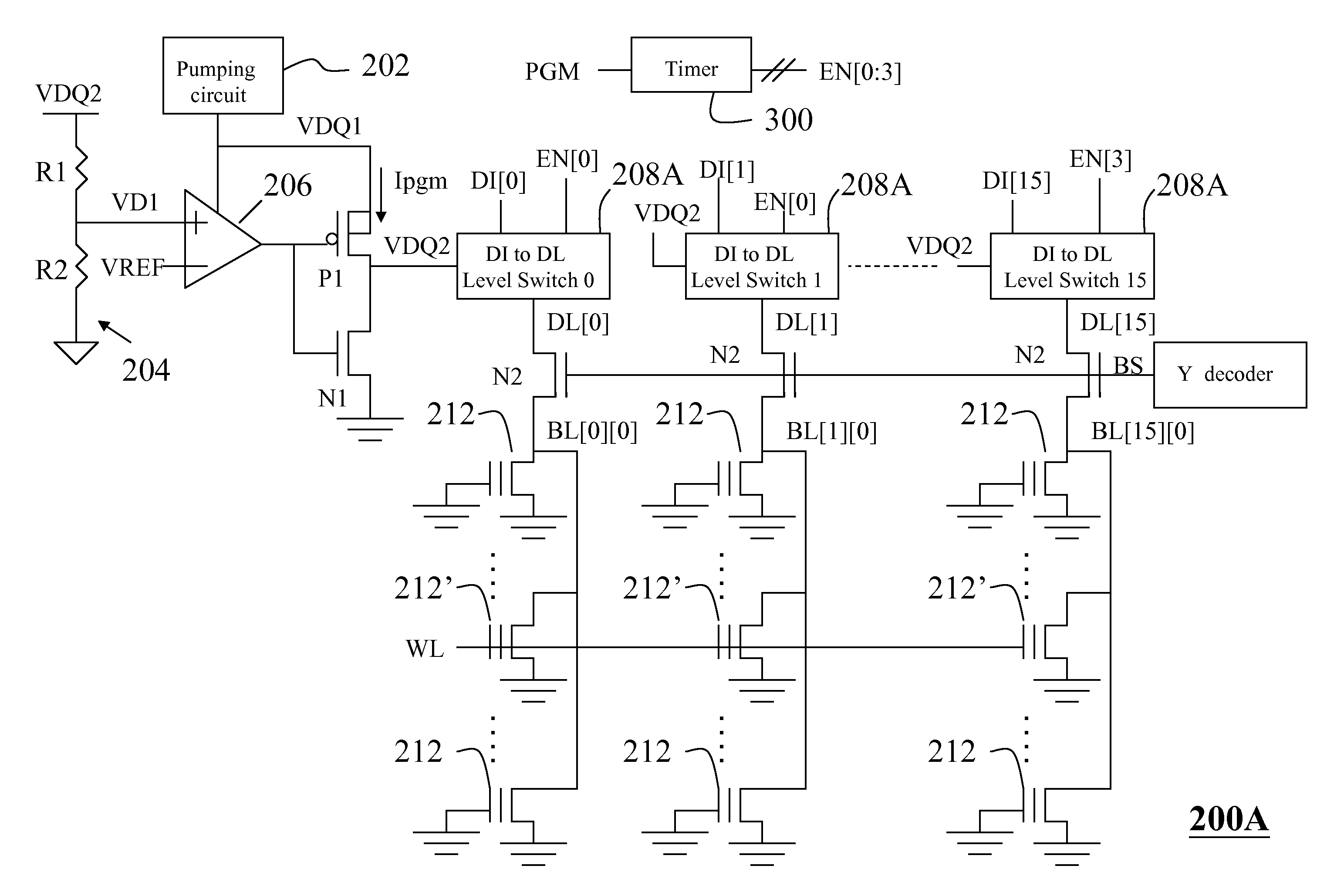
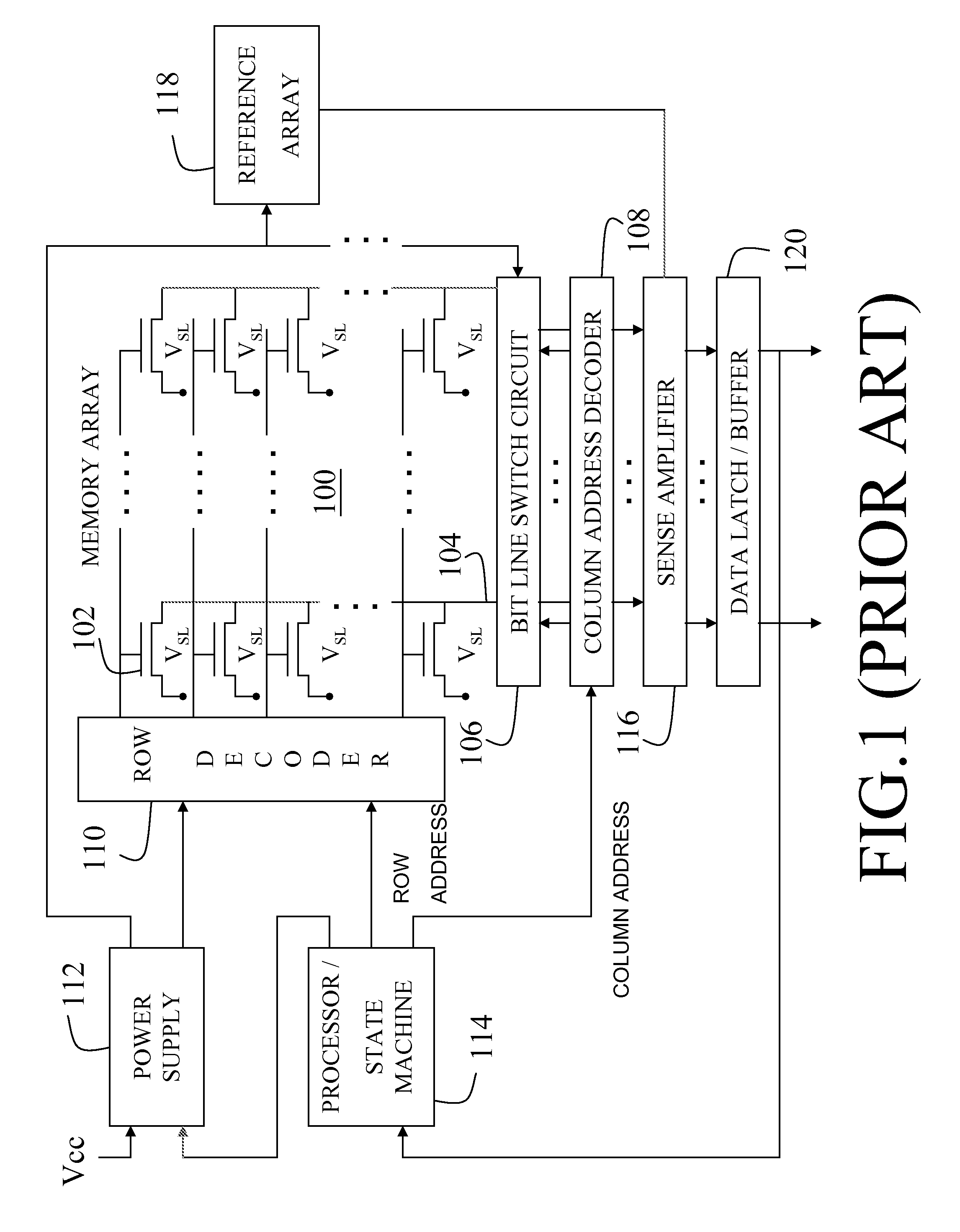
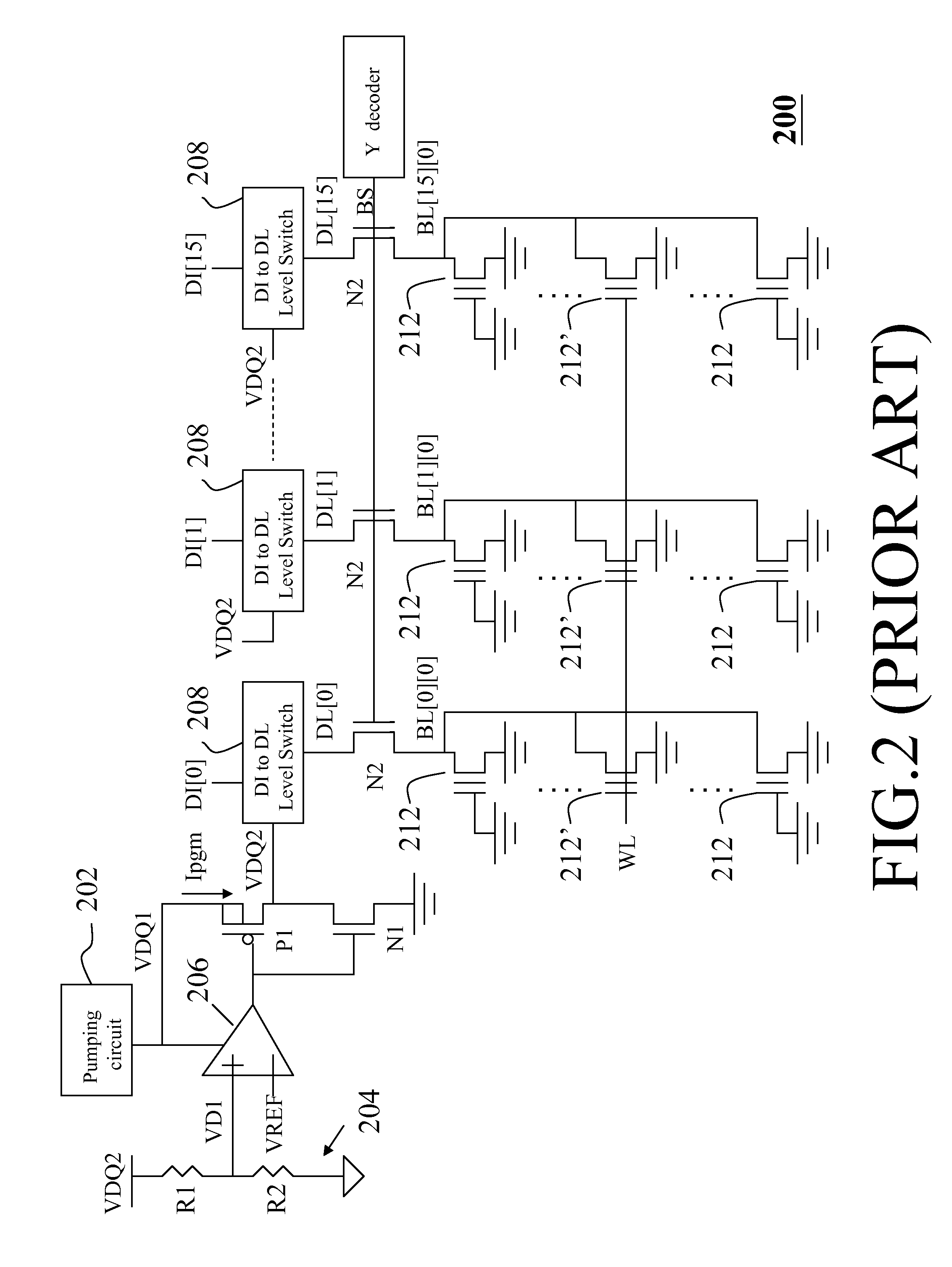
[0022]FIG. 2 is a circuit diagram of a prior art programming circuit 200 for programming memory cells of a semiconductor memory device, such as the flash memory device of FIG. 1 including an array of NOR memory cells, hereinafter sometimes referred to as a “flash memory device.” Those features of the flash memory device not described herein are known to those of ordinary skill in the art and need not be repeated herein. Commonly assigned U.S. Pat. No. 7,009,882 provides a detailed discussion of the flash memory device structure, the entirety of which is hereby incorporated by reference herein.

[0023]The programming device 200 includes a power supply, such as charge pump circuit 202, that provides voltage value VDQ1. Various structures for charge pump circuit 202 are known in the art. Generally, charge pumps use capacitors as energy storage elements and some form of switching device to control connection of voltages to the capacitor. The pump circuit may also include an output capacit...


PUM


Abstract

A method of programming a group of memory cells in a semiconductor memory device selecting a group of memory cells for programming, and enabling a first subgroup of memory cells from the group of memory cells for programming. After enabling the first subgroup, the programming method waits a first predetermined time period and after the first predetermined time period, enables a second subgroup of memory cells from the group of memory cells for programming while continuing to enable the first subgroup for programming.

Description

FIELD OF THE INVENTION[0001]The present invention relates to memory devices and more specifically to flash memory devices and methods of programming the same.BACKGROUND OF THE INVENTION[0002]FIG. 1 shows a typical configuration for an integrated circuit including a flash EEPROM (electrically erasable and programmable ROM) memory array 100 and circuitry enabling programming, erasing, reading, and overerase correction for memory cells in the array 100. The flash EEPROM array 100 is composed of individual flash memory cells, such as cell 102. Each cell 102 has a drain connected to a bit line, such as bit line 104, each bit line being connected to a bit line switch circuit 106 and column decoder 108. Sources of the array cells are connected to each other and VSL, which is the common source signal, while their gates are each connected by a word line to a row decoder 110.[0003]The row decoder 110 receives voltage signals from a power supply 112 and distributes the particular voltage signa...

Claims


Application Information

Patent Timeline
Patent Type & Authority Patents(United States)
IPC IPC(8): G11C7/10
CPCG11C16/10G11C16/12
Inventor CHEN, CHUNG-ZEN
Owner ELITE SEMICON MEMORY TECH INC
Why Eureka
Try Eureka