Method and apparatus for testing semiconductor memory device and related testing methods

a technology of memory devices and semiconductors, applied in the direction of measurement devices, error detection/correction, instruments, etc., can solve the problems of increasing the duration of certain test times, and increasing the time required to test conventional semiconductor memory devices

Active Publication Date: 2008-12-09
SAMSUNG ELECTRONICS CO LTD
View PDF9 Cites 6 Cited by
  • Summary
  • Abstract
  • Description
  • Claims
  • Application Information

AI Technical Summary

Problems solved by technology

However, these conventional test methods cannot be applied to a network of Dynamic Random Access Memory (DRAM) because the DRAM typically include at least some memory cells storing parity information.
Additionally, the time required to test conventional semiconductor memory devices tends to rise as the number of data pins on the devices increases.
Given the trend towards higher pin counts, the duration of certain test times is becoming an issue.
In sum, the conventional apparatuses and methods applied to the testing of semiconductor memory devices result in unacceptably long test times. Test times must be further reduced without increasing or otherwise altering the then number of data pins associated with the semiconductor memory devices.

Method used


Image

  • Method and apparatus for testing semiconductor memory device and related testing methods
  • Method and apparatus for testing semiconductor memory device and related testing methods
  • Method and apparatus for testing semiconductor memory device and related testing methods

Examples


Embodiment Construction

[0031]Exemplary embodiments of the present invention are set forth below with reference to the accompanying drawings.

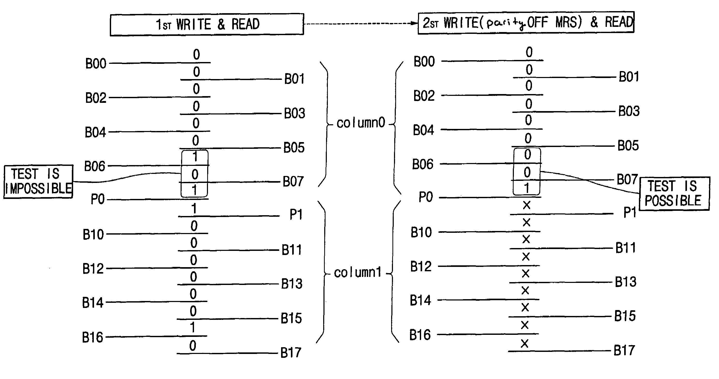
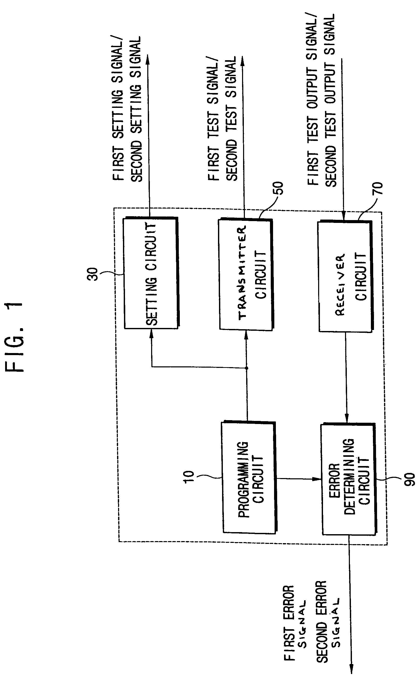
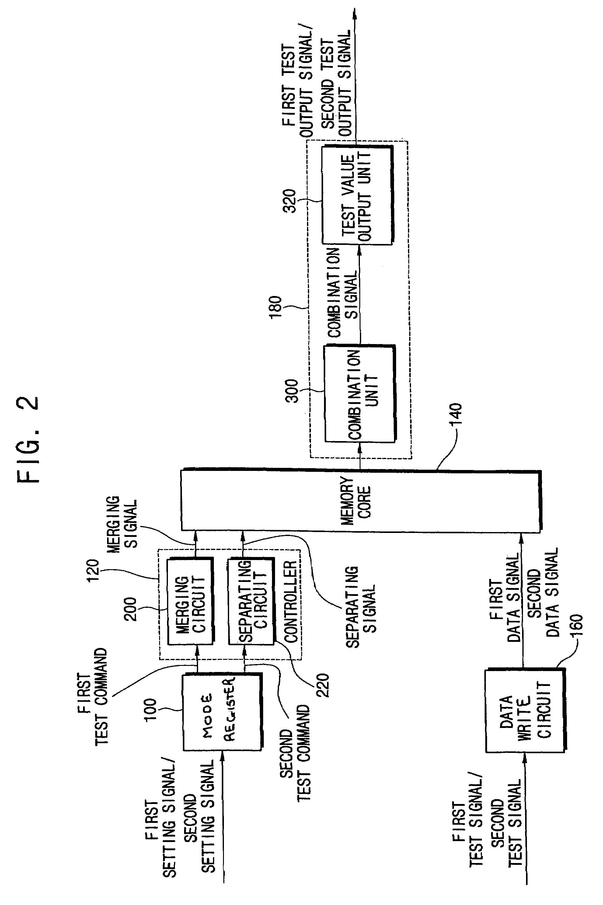
[0032]FIG. 1 is a block diagram showing an apparatus for testing semiconductor memory device according to one exemplary embodiment of the present invention. Referring to FIG. 1, the apparatus for testing semiconductor memory device generally comprises a programming circuit 10, a setting circuit 30, a transmitter circuit 50, a receiver circuit 70, and an error detection circuit 90.

[0033]Programming circuit 10 is adapted to program a related test apparatus in a first test mode and / or a second test mode. More specifically, programming circuit 10 first programs the test apparatus in the first test mode, and thereafter performs a test in the first test mode. After waiting a predetermined period following execution of the first test mode, programming circuit 10 re-programs the test apparatus in the second test mode, and the thereafter performs another test in the second tes...


PUM


Abstract

A test method and apparatus for a semiconductor memory device is characterized by the sequentially programmed use of two test different modes. A first test mode tests at least signal line integrity for the semiconductor memory device by testing a merged set of bits line. The second test mode further tests at least signal line integrity after first separating the merged bits lines. Logical combination of test data derived from the first and second test modes are used to generate error detection signals. At least one bit line associated with a parity bit is preferable merged and separated in the foregoing approach.

Description

BACKGROUND OF THE INVENTION[0001]1. Field of the Invention[0002]The present invention relates generally to a method and apparatus for testing a semiconductor memory device. The present invention also related to a semiconductor memory device adapted to testing in a reduced testing time.[0003]A claim to priority is made to Korean Patent Application No. 2003-88677 filed on Dec. 8, 2003, the subject matter of which is incorporated by reference.[0004]2. Description of the Related Art[0005]The typical apparatus for testing a semiconductor memory device incorporates several different methods to test for various failures in the device. One test method commonly run is the parallel bit test (PBT). The PBT tests a plurality of memory cells using only a small number of data pins. A conventional semiconductor memory device typically includes an even number of memory cells on every column, and an even number of data pins. Thus, conventional methods for testing such a semiconductor memory device e...

Claims


Application Information

Patent Timeline
Patent Type & Authority Patents(United States)
IPC IPC(8): G11C29/00G11C7/00G11C29/12
CPCG11C29/12G11C2029/1204G11C2029/2602G11C29/00
Inventor SEO, SEONG-YOUNG
Owner SAMSUNG ELECTRONICS CO LTD
Why Eureka
Try Eureka