Method of determining quasi-phase matching efficiency in periodically poled structure of optical waveguide, periodically poled structure of optical waveguide, and optical waveguide using the same
a technology of periodic pole structure and quasi-phase matching efficiency, which is applied in the direction of optical waveguide light guide, optical light guide, etc., can solve the problems of severe poling efficiency decline, and achieve the effect of increasing quasi-phase matching efficiency and maximizing the conversion efficiency of non-linear optical phenomena
- Summary
- Abstract
- Description
- Claims
- Application Information
AI Technical Summary
Benefits of technology
Problems solved by technology
Method used
Image
Examples
first embodiment
[0042
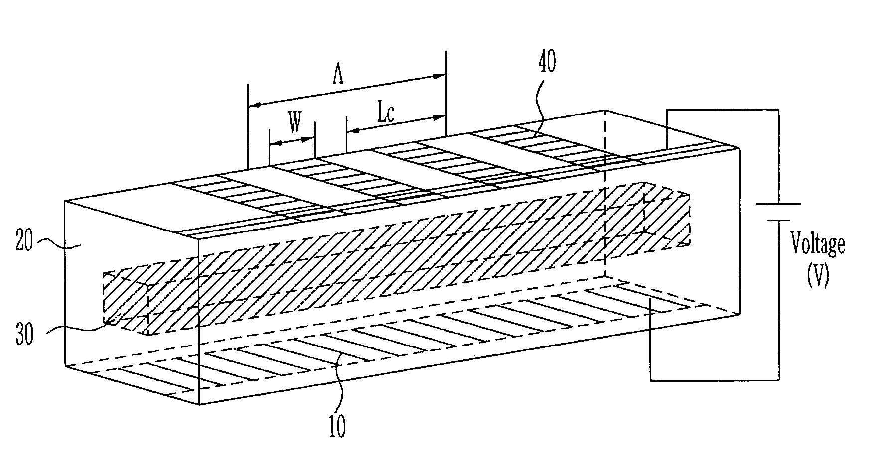
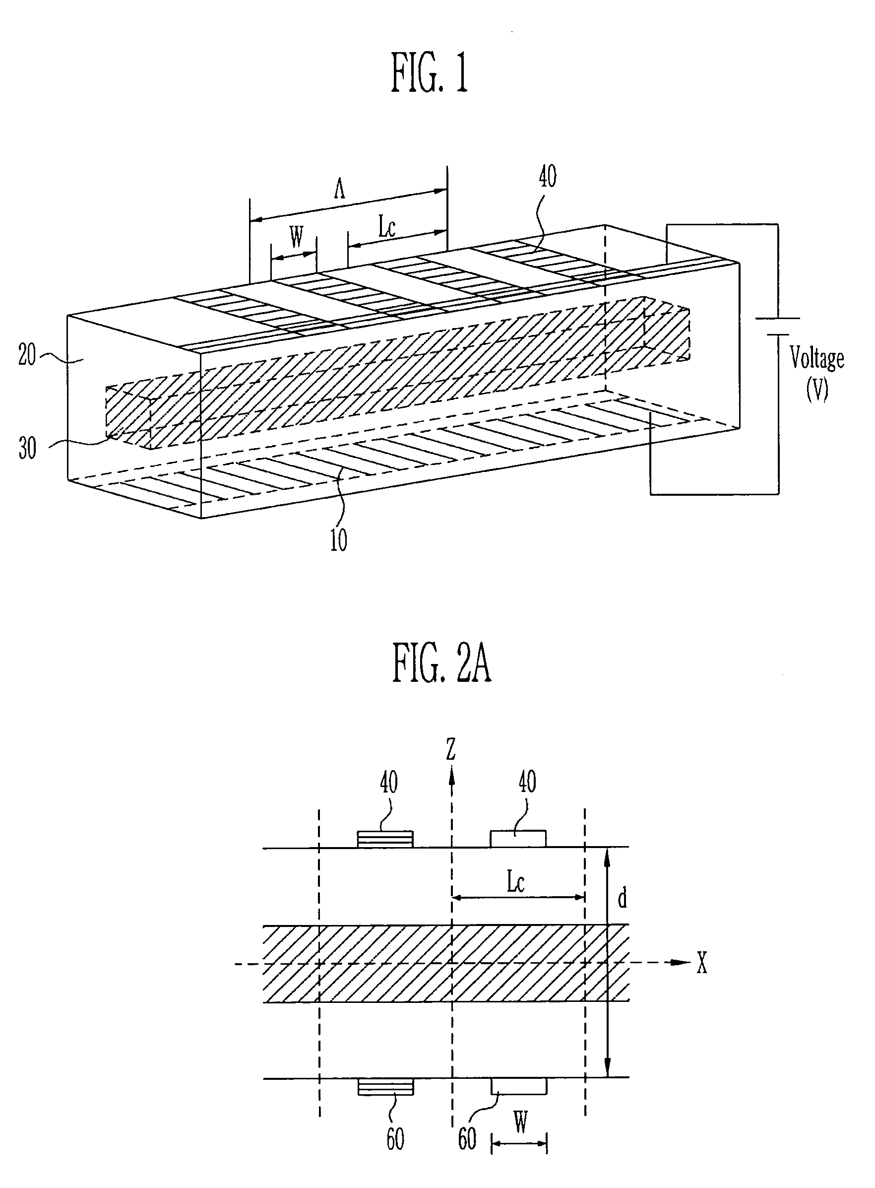
[0043]FIG. 2A is a schematic view showing the periodically poled structure of the optical waveguide according to the first embodiment of the present invention. The period electrodes 40, 60 are arranged at an interval of coherence lengths Lc by every two pairs on both surfaces of the optical waveguide, where each pair of periodic electrodes are spaced by the distance d between electrodes which is a sum of the thickness of the core and the cladding. The electrode width w satisfies 0
[0044]FIG. 2A is a view showing the poling structure in which electric fields of opposite direction are applied to each pair of the periodic electrodes. Assuming that an electrical interaction is not generated between the periodic electrodes in each pair, the distribution of the electric field due to the two pairs of the periodic electrodes can be represented by linear combination of the electric fields due to each pair of the periodic electrodes. Since the pulse poling structure for alternately ...
second embodiment
[0069
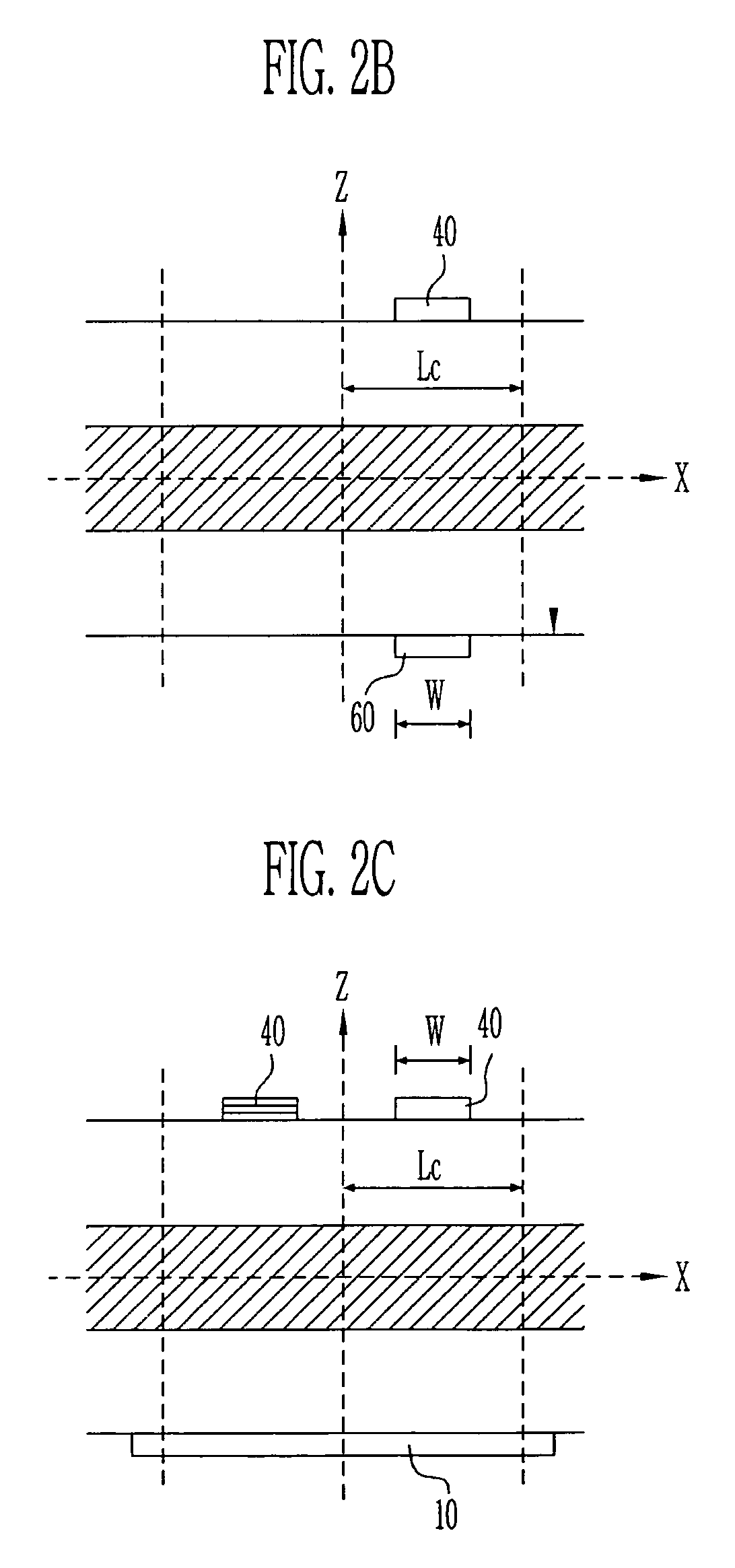
[0070]FIG. 2B is a view schematically showing the periodically poled structure of the optical waveguide according to the second embodiment of the present invention. In this structure, the periodic electrodes 40, 60 are arranged at an interval of 2 Lc at both sides of the optical waveguide. Due to the translation symmetric of the electrode structure, the origin of the coordinates system is placed on a center of one period to have a center of a pair electrodes at a place of x=Lc / 2. Accordingly, if a DC voltage is applied to the electrode paced at 0≦x≦Lc, then the electric field of one pattern is generated. The mainly different point in comparison with the first embodiment is that in the case of the poling state, one pair of electrodes does not exist every period, and a normalized DC poling instead of the pulse poling can be used. The mean distribution of the periodically poled structure according to the second embodiment is calculated on the basis of the basis electric field simi...
third embodiment
[0075](Third Embodiment)
[0076]FIG. 2C is a view schematically showing the periodically poled structure of the optical waveguide according to the third embodiment of the present invention. On one surface of the optical waveguide, the period electrode 40 is arranged at an interval of Lc, and on the other surface of the optical waveguide, a long flat electrode 10 is arranged. The poling structure in the third embodiment is matched to the poled structure of the first embodiment with the exception the fact that a continuously flat electrode is employed instead of the series periodic electrode placed at one surface. In this structure, assuming that the basis electric field has a form of Eb(x,w,2d), other calculations can be easily performed by using the case of d->2d instead of the result of the first embodiment. The distribution of the electric field in an nth period is represented as follows:
[0077]EnIII(x,w,d)=Eb(x-nΛ-Lc2,w,2d)-Eb(-x+nΛ-Lc2,w,2d).(10)
[0078]Accordingly, the whol...
PUM
| Property | Measurement | Unit |
|---|---|---|
| quasi-phase | aaaaa | aaaaa |
| width | aaaaa | aaaaa |
| coherence length | aaaaa | aaaaa |
Abstract
Description
Claims
Application Information


