Vertical integration of active devices within passive semiconductor waveguides

a semiconductor waveguide and active device technology, applied in the direction of optical waveguide light guide, optical element, instrument, etc., can solve the problems of inability to meet the requirements of the application, so as to improve the manufacturability

Inactive Publication Date: 2006-08-22
ENABLENCE
View PDF11 Cites 44 Cited by
  • Summary
  • Abstract
  • Description
  • Claims
  • Application Information

AI Technical Summary

Problems solved by technology

While simple engineering solutions resulting in hybrid components are functionally attractive for some applications, they may be prohibitively cumbersome and costly for others.
The former is straightforward but expensive and unreliable due to its difficulty in implementation, since it requires complex epitaxial growth techniques such as etch and re-growth, e.g. reported by S. Lourdudoss et al, in “Uniqueness of Hydride Vapour Phase Epitaxy in Optoelectronic Device Fabrocation”, Int. Conf. Indium Phosphide and Related Materials, May 11–15 May 1998, Tsukuba, Japan, P.
The latter uses simple single-step epitaxial growth, but has problems with coupling efficiency between passive and active waveguides, when the active waveguide is grown on top of the passive one.
However, none of them are both simple to implement and cost efficient at present and hence these approaches also do not solve the problem of developing reliable and inexpensive integrated devices for sale and distribution in the very near term.

Method used


Image

  • Vertical integration of active devices within passive semiconductor waveguides
  • Vertical integration of active devices within passive semiconductor waveguides
  • Vertical integration of active devices within passive semiconductor waveguides

Examples


example

Integrated Semiconductor Optical Amplifier

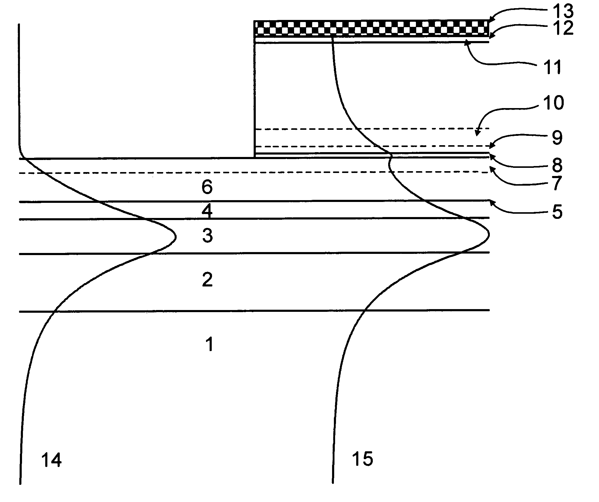
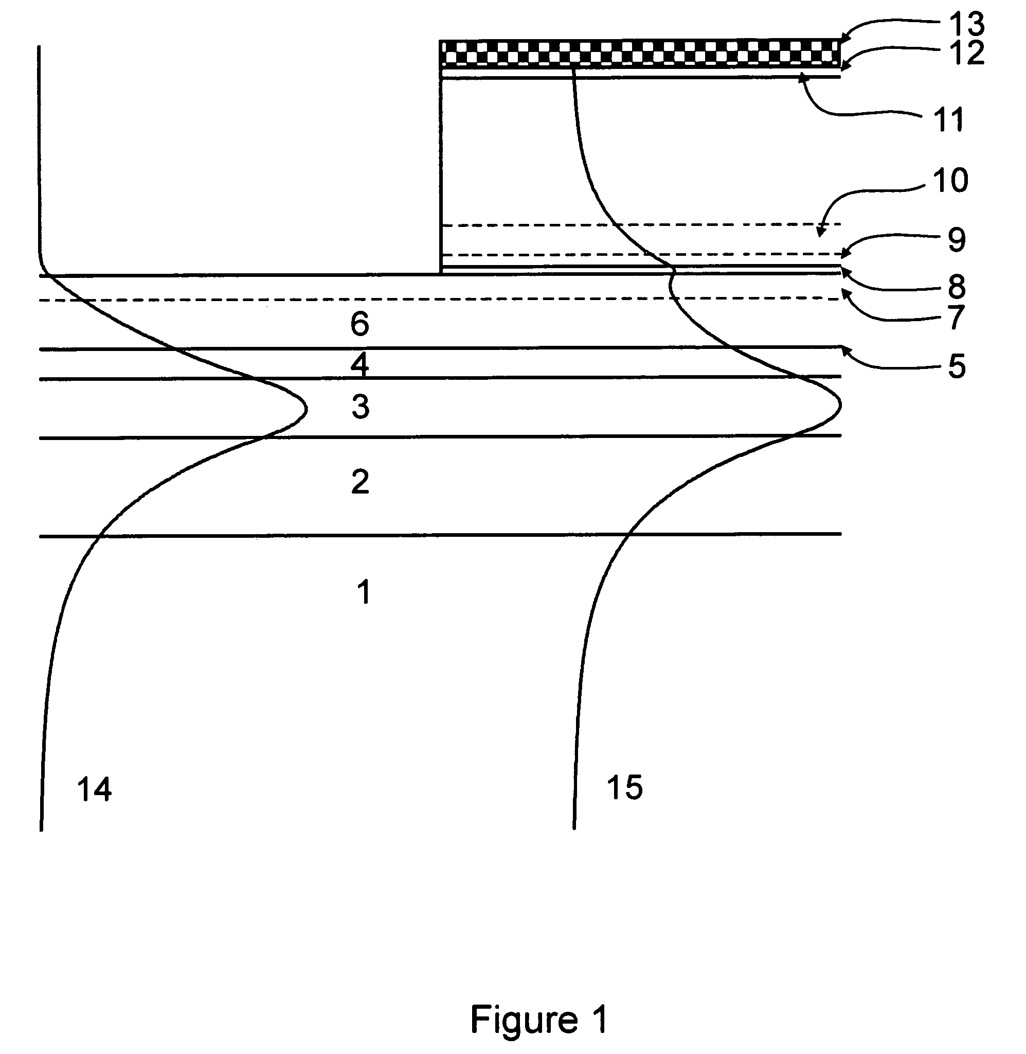
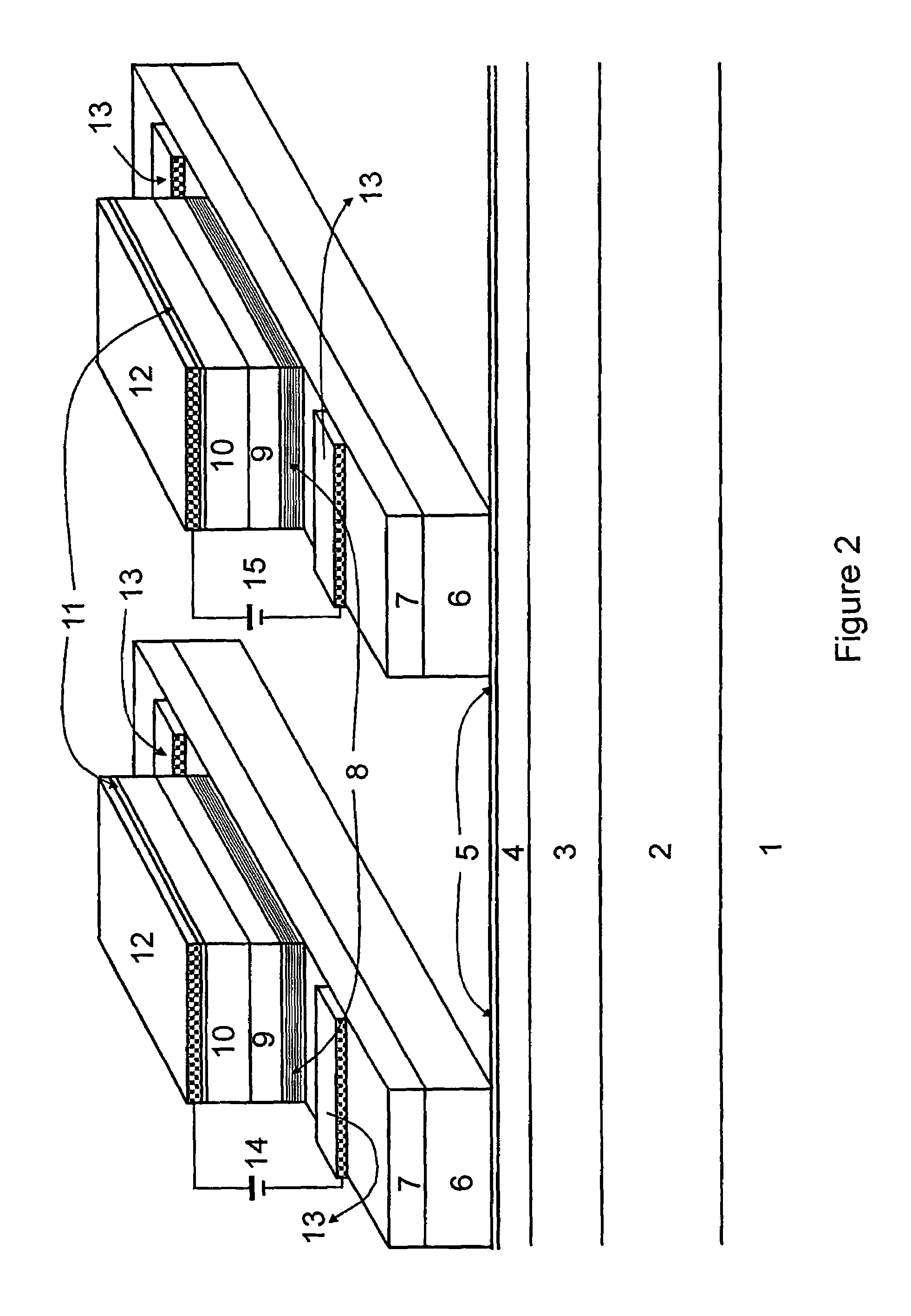
[0047]Another exemplary embodiment of the invention, in the form of a monolithically integrated SOA having the layer structure specified in Table III and the device layout illustrated in FIG. 4, is described. The distribution of the vertical mode field in the passive and active waveguide portions is close to that shown in FIG. 6 for the embodiment in the form of the EAA with the layer structure of Table IIB. The layer structure of the integrated SOA is similar to that of the integrated EAA, with the only difference being in the material of the active layer 8. As in the case of the EAA, it is optionally either bulk or QW material, in any event having a bandgap energy close to operating photon energy, Eg≈h-ω. In a particular embodiment with the layer structure given in Table III, the stack of 5 16-nm tensile-strained lnGaAs wells and 6 36.6-nm unstrained GaInAsP layers having a bandgap wavelength of 1.0 μm, i.e. the same as that in the quatern...


PUM


Abstract

The invention discloses a method for monolithic integration of active devices within passive semiconductor waveguides and the application of this method for use in InP-based planar wavelength division multiplexing components of optical communication systems. The epitaxial device is grown in a single run and comprises a number of layers, such that the lower part of the structure acts as a single mode passive waveguide while the upper part of the structure contains a planar PIN diode. The PIN structure is present only in the active waveguide portion and absent in all the passive waveguide portions. The active and passive waveguide portions have substantially similar guiding properties with the exception of a mode tail above a top surface of the passive waveguide portion within the active waveguide portion. As a result, an optical signal portion penetrates the I-layer of the PIN structure and interacts with semiconductor material therein for actively affecting an intensity of the optical signal with no substantial changes in guiding properties of the semiconductor waveguide. Embodiments of invention in the form of monolithically integrated waveguide photodetector, electro-absorptive attenuator and semiconductor optical amplifier are disclosed in terms of detailed epitaxial structure, layout and performance characteristics of the device.

Description

[0001]This application claims the benefit of U.S. Provisional Application No. 60 / 278,750, filed Mar. 27, 2001.FIELD OF THE INVENTION[0002]The invention relates generally to monolithic integration of active semiconductor devices onto passive waveguides of planar wavelength division multiplexing (WDM) components and more particularly to waveguide photodetectors (WPD), electro-absorptive attenuators (EAA) and semiconductor optical amplifiers (SOA), all having a PIN structure on top of a passive seiniconductor waveguide and, in use, acting as a single-mode waveguide device with either 1) high-efficiency photodetection, due to direct interband transitions in the I-layer of a reverse-biased PIN structure, or 2) variable optical attenuation, due to interband electro-absorption in the I-layer of a reverse-biased PIN structure, or 3) variable optical amplification, due to stimulated radiative recombination of carriers injected into the I-layer of a forward-biased PIN structure.BACKGROUND OF ...

Claims


Application Information

Patent Timeline
Patent Type & Authority Patents(United States)
IPC IPC(8): G02B6/10G02B6/12H01L31/105
CPCG02B6/12004H01L31/105G02B2006/12123G02B2006/12126G02B2006/12164G02B2006/12178G02B2006/12142
Inventor TOLSTIKHIN, VALERY I.
Owner ENABLENCE
Why Eureka
Try Eureka