Electronic ballast with lossless snubber capacitor circuit

a capacitor circuit and electronic ballast technology, applied in the direction of electric variable regulation, process and machine control, instruments, etc., can solve the problems of damage to the capacitive mode switching, the open circuit voltage of the instant-start ballast needs to be controlled, and the high circulating current, so as to reduce the loss of turn off and limit the variation of output voltage

Inactive Publication Date: 2006-08-29
UNIVERSAL LIGHTING TECHNOLOGIES
View PDF24 Cites 7 Cited by
  • Summary
  • Abstract
  • Description
  • Claims
  • Application Information

AI Technical Summary

Benefits of technology

[0007]A preferred embodiment of the present invention is directed toward an electronic ballast for producing an output voltage on a pair of output terminals for igniting and powering a gas discharge lamp connected between the output terminals. The ballast includes an inverter having a pair of transistors. A snubber circuit reduces turn off losses in the transistors. The snubber circuit includes a pair of series connected snubber capacitors connected in parallel with the pair of transistors. An extended dead time is created between gating signals of the pair of transistors to allow the snubber capacitors to discharge. The electronic ballast includes a resonant tank having a series connected tank inductor and tank capacitor and an output voltage sensing circuit that senses an output voltage of the ballast by sensing a voltage across a sampling capacitor connected in series with the tank capacitor. An open circuit voltage control circuit is also preferably included that controls a voltage across the output terminals when a gas discharge lamp is not connected between the output terminals. The open circuit voltage control circuit includes a resistor connected in series with a tank capacitor of the ballast. A cable compensation circuit is also preferably included that limits variations in the output voltage of the electronic ballast due to a cable being connected to the output terminals of the ballast. The cable compensation circuit limits variations in the output voltage by altering the gating signals provided to the transistors.
[0008]Another embodiment of the present invention is directed toward an electronic ballast for providing an output voltage on a pair of output terminals for use in powering a gas discharge lamp. The ballast includes an inverter circuit having a first transistor and a second transistor and a resonant tank having a tank capacitor and a tank inductor. A substantially lossless snubber circuit reduces turn-off losses in the first and second transistors of the inverter. The snubber circuit includes a snubber capacitor connected in parallel with each of the first transistor and the second transistor. A microcontroller provides gating signals to the transistors such that an extended dead time is created between the gating signals of the transistors to allow the snubber capacitors to discharge. An open circuit voltage control circuit controls a voltage across the output terminals of the ballast when a gas discharge lamp is not connected between the output terminals. A sampling capacitor connected in series with the tank capacitor wherein an output voltage of the ballast is sampled across the sampling capacitor.
[0009]Yet another embodiment of the present invention is directed toward an electronic ballast having a half-bridge inverter circuit that includes a pair of transistors and a pair of capacitors. Each capacitor is connected in parallel with one of the transistors. A microcontroller generates transistor switching control signals that cause the transistors to switch on and off at a rate that allows the capacitors to reduce turn off losses in the transistors. This is preferably accomplished by creating an extended dead time between the gating signals of the pair of transistors that allows the capacitors to discharge. The electronic ballast has a resonant tank having a series connected tank inductor and tank capacitor. A sampling capacitor is connected in series with the tank capacitor wherein an output voltage of the ballast is sampled across the sampling capacitor. An open circuit voltage control circuit is also included that controls a voltage across the output terminals of the ballast when a gas discharge lamp is not connected between the output terminals. The open circuit voltage control circuit has a resistor connected in series with the sampling capacitor and the voltage across the resistor is used to limit the output voltage of the electronic ballast. A cable compensation circuit is also preferably provided to limit variations in the output voltage due to cables being connected to outputs of the ballast.

Problems solved by technology

One problem with prior art electronic ballasts is that the open circuit voltage of an instant-start ballast needs to be controlled when there is not a lamp coupled to the ballast.
Unfortunately, prior art methods of providing this open circuit voltage control cause substantial variations in the open circuit voltage when used in conjunction with different lengths of cable, or require a high value resonant capacitor which results in a high circulating current.
A high circulating current is undesirable in that it increases the conduction losses in the ballast and may result in damaging capacitive mode switching occurring during the striking transients.
As a result, large open circuit voltage variations often result when external connections to the fixture, such as a connecting cable, add extra capacitance.
However, potentially damaging hard switching or capacitive mode switching is often observed in these high capacitance types of prior art open circuit voltage controlled ballasts.
Furthermore, the use of a large resonant capacitor makes the resonant tank difficult to design.
As a result, these types of ballasts suffer from more conduction losses and / or hard switching during the striking of the lamp than do typical ballasts.
Conduction losses and hard switching are undesirable in that they may cause the ballast to fail.
The result is undesirable hard switching occurring during the striking.
However, these circuits are often complex and decrease the efficiency, while increasing the cost, of the ballast.

Method used


Image

  • Electronic ballast with lossless snubber capacitor circuit
  • Electronic ballast with lossless snubber capacitor circuit
  • Electronic ballast with lossless snubber capacitor circuit

Examples


Embodiment Construction

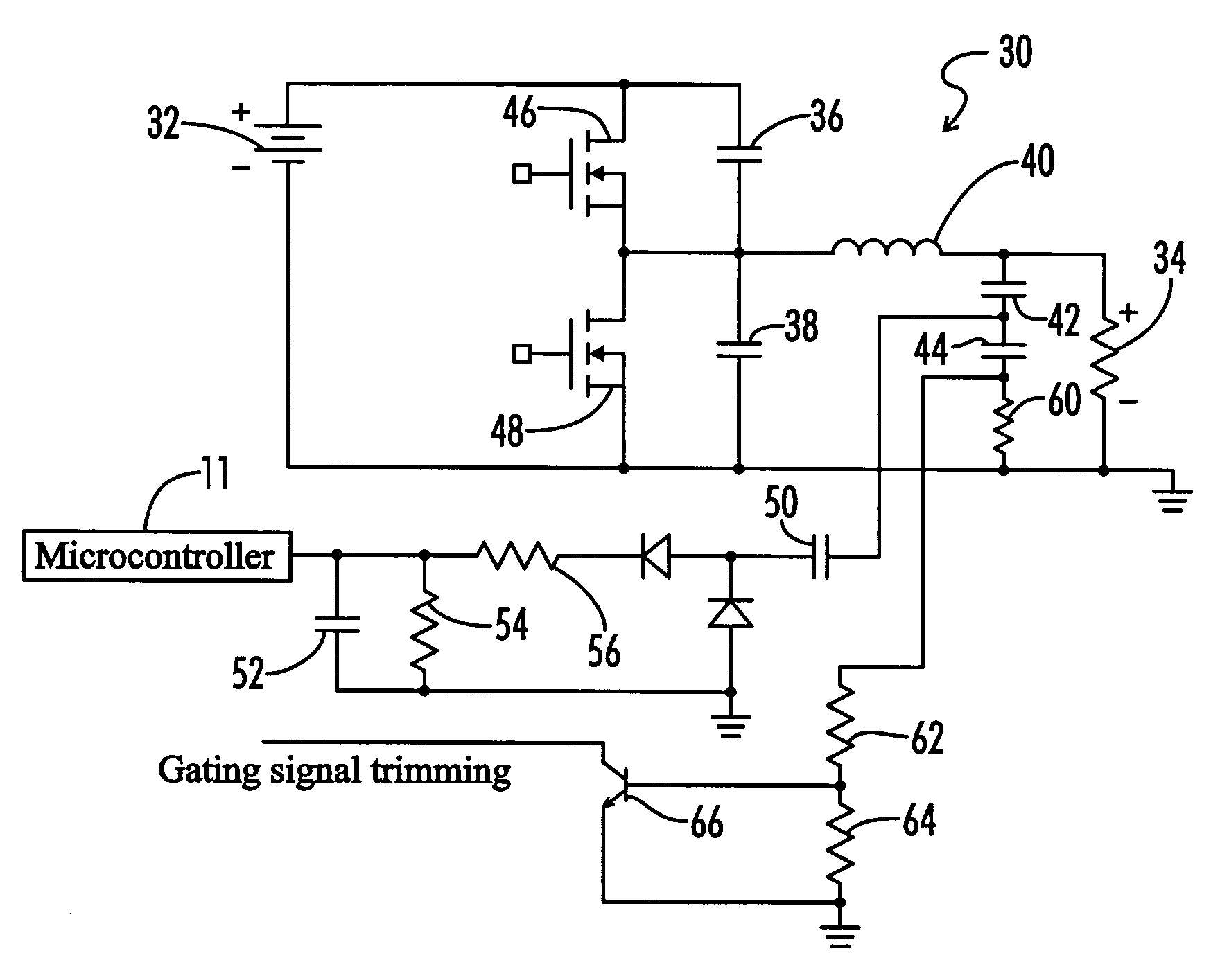
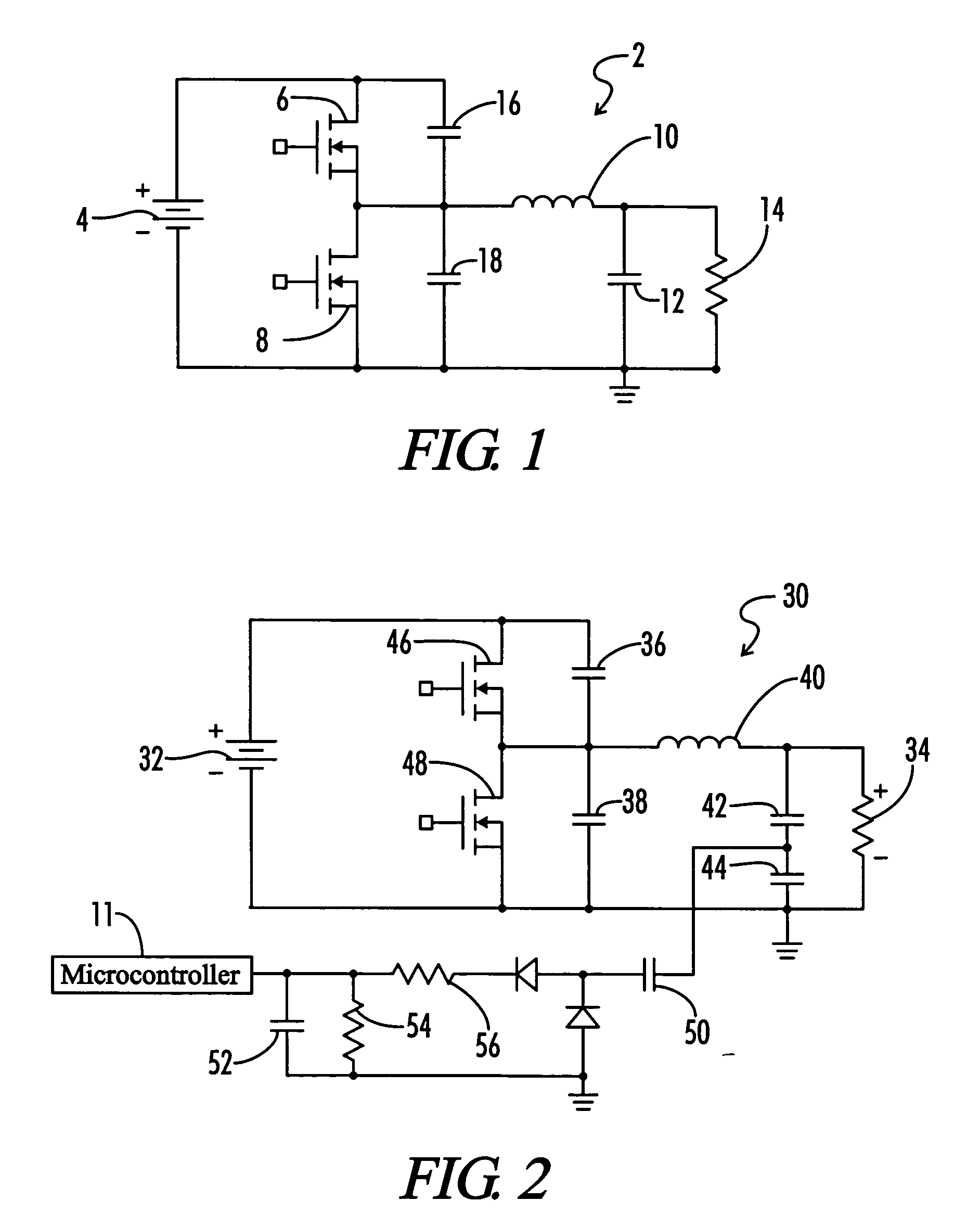
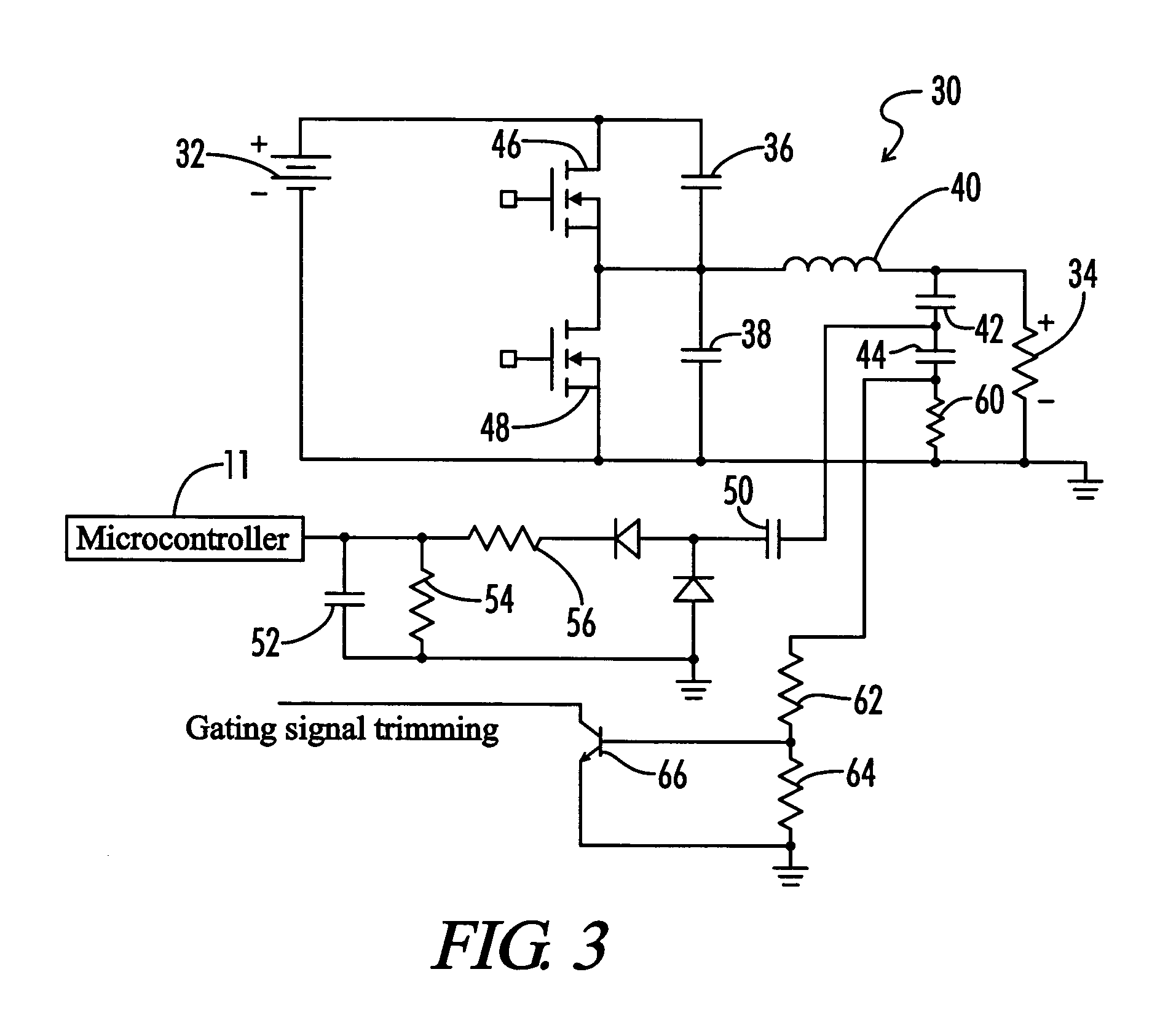
[0014]A preferred embodiment of the present invention is directed toward an instant start electronic ballast for a gas discharge lamp having a substantially lossless snubber circuit for reducing the turn off loses of the transistors in the inverter of the ballast. For voltage-fed, series-resonant, half-bridge inverters, the turning-on of the FETS or transistors involves zero voltage switching, but the turning-off of the FETS and transistors involves hard switching. For most ballasts, the turning-off current is small so that losses associated with the turning-off are not significant. However, for an Instant Start—High Range Voltage ballast, the current at turn-off is near its peak and, thus, the turn-off losses are relatively high. Furthermore, due to the larger die size of the high voltage FETS, more gate charge has to be removed from the gates before they can be turned-off. This increased gate charge increases the turn-off losses for a high voltage inverter.

[0015]A simplified schem...


PUM


Abstract

An improved high input voltage instant start electronic ballast uses a substantially lossless snubber circuit. The substantially lossless snubber circuit is incorporated into the ballast to reduce turn off losses and increase the efficiency of the ballast. The snubber circuit includes two capacitors connected in parallel with respect to the two switching transistors or FETS in the inverter of the ballast. A series-resonant lamp voltage sensing circuit is also provided that uses a voltage dividing capacitor to accomplish lossless monitoring of the open circuit voltage of the ballast. A cable compensation circuit minimizes variations in the open circuit voltage due to the connecting and disconnecting of a cable to the ballast by limiting the turn on times of the transistors during high voltage conditions.

Description

CROSS-REFERENCES TO RELATED APPLICATIONS[0001]This application is a Non-Provisional Utility application which claims benefit of co-pending U.S. patent application Ser. No. 60 / 526,638 filed Dec. 3, 2003, entitled “High Input Voltage Microcontroller Based Instant Start Ballast” which is hereby incorporated by reference.STATEMENT REGARDING FEDERALLY SPONSORED RESEARCH OR DEVELOPMENT[0002]Not ApplicableREFERENCE TO SEQUENCE LISTING OR COMPUTER PROGRAM LISTING APPENDIX[0003]Not ApplicableBACKGROUND OF THE INVENTION[0004]One problem with prior art electronic ballasts is that the open circuit voltage of an instant-start ballast needs to be controlled when there is not a lamp coupled to the ballast. Unfortunately, prior art methods of providing this open circuit voltage control cause substantial variations in the open circuit voltage when used in conjunction with different lengths of cable, or require a high value resonant capacitor which results in a high circulating current. A high circul...

Claims


Application Information

Patent Timeline
Patent Type & Authority Patents(United States)
IPC IPC(8): H05B37/02H05B37/00H05B41/00H05B41/14H05B41/285H05B41/36
CPCH05B41/2828H05B41/2851Y10S315/07Y02B20/186Y02B20/00
Inventor YU, QINGHONGRADZINSKI, CHRISTOPHERDERNOVSEK, JOHN JAYSHACKLE, PETER
Owner UNIVERSAL LIGHTING TECHNOLOGIES
Why Eureka
Try Eureka