

Switching circuit and semiconductor device
a technology of switching circuit and semiconductor device, which is applied in the direction of electronic switching, pulse technique, power conversion system, etc., can solve the problems of difficult reduction of the gate resistance, insatisfactory relationship between the switching speed and the turn-off loss, and inability to reduce the turn-off loss of the igbt in a low current phase. , to achieve the effect of reducing the load of the first igbt and the second igbt, reducing th
- Summary
- Abstract
- Description
- Claims
- Application Information
AI Technical Summary
Benefits of technology
Problems solved by technology
Method used
Image

Examples
first embodiment
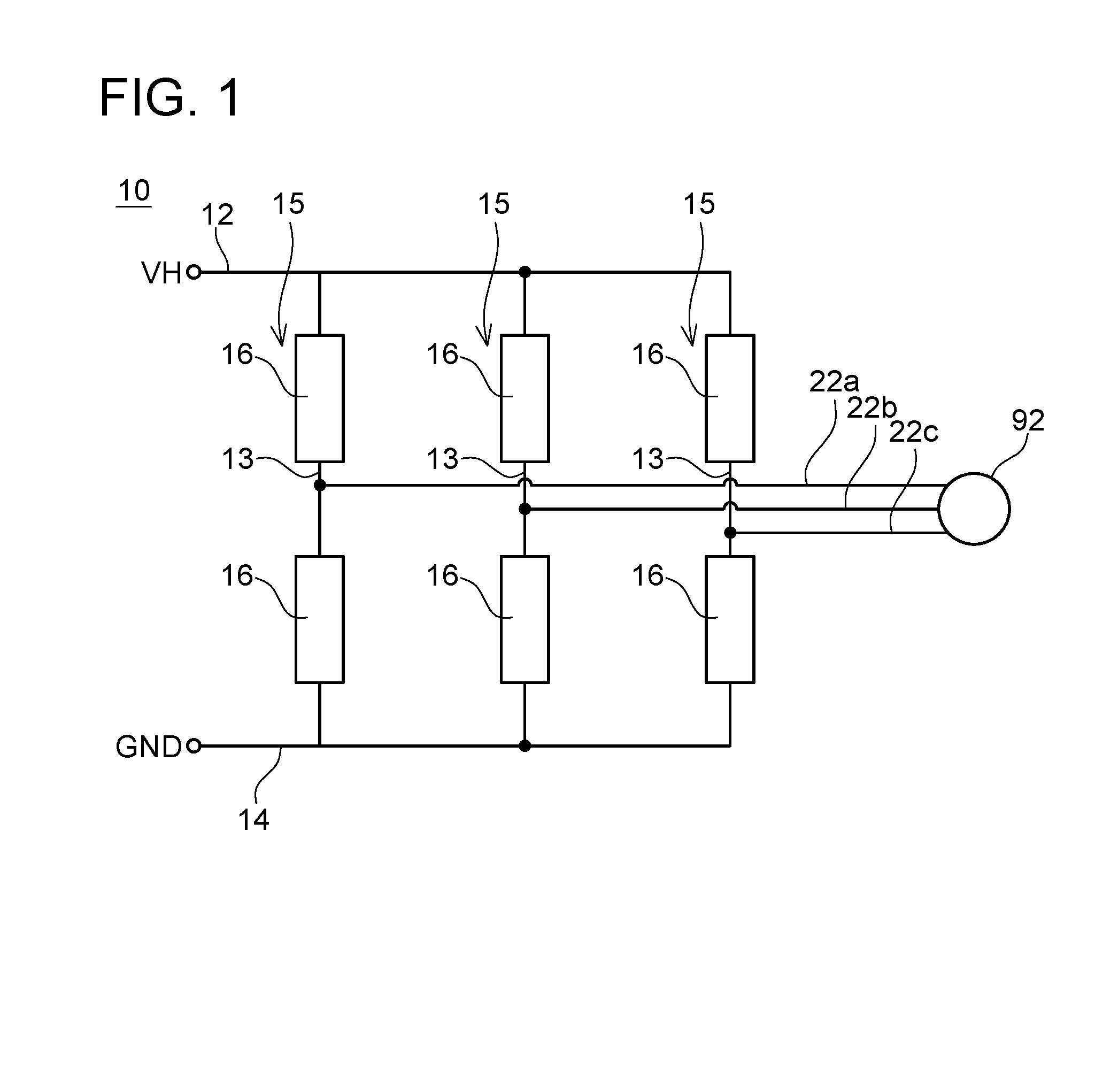
[0022]The inverter circuit 10 of the first embodiment, shown in FIG. 1, supplies an alternating current to a motor 92. The inverter circuit 10 has a high-potential wiring 12 and a low-potential wiring 14. The high-potential wiring 12 and the low-potential wiring 14 are connected to a direct-current power source that is not illustrated. A positive potential VH is applied to the high-potential wiring 12, and a ground potential (0 V) is applied to the low-potential wiring 14. Three series circuits 15 are connected in parallel with each other between the high-potential wiring 12 and the low-potential wiring 14. Each of the series circuits 15 has a connecting wiring 13, which is connected between the high-potential wiring 12 and the low-potential wiring 14, and two switching circuits 16 interposed in the connecting wiring 13. The two switching circuits 16 are connected in series between the high-potential wiring 12 and the low-potential wiring 14. Output wirings 22a to 22c are connected ...
second embodiment
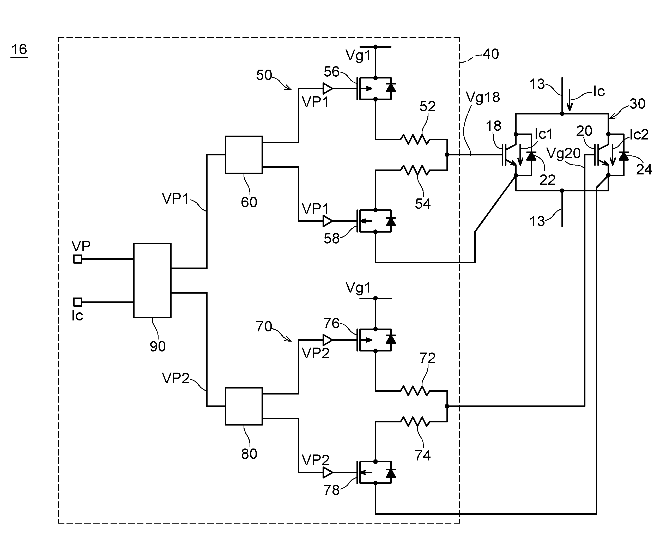
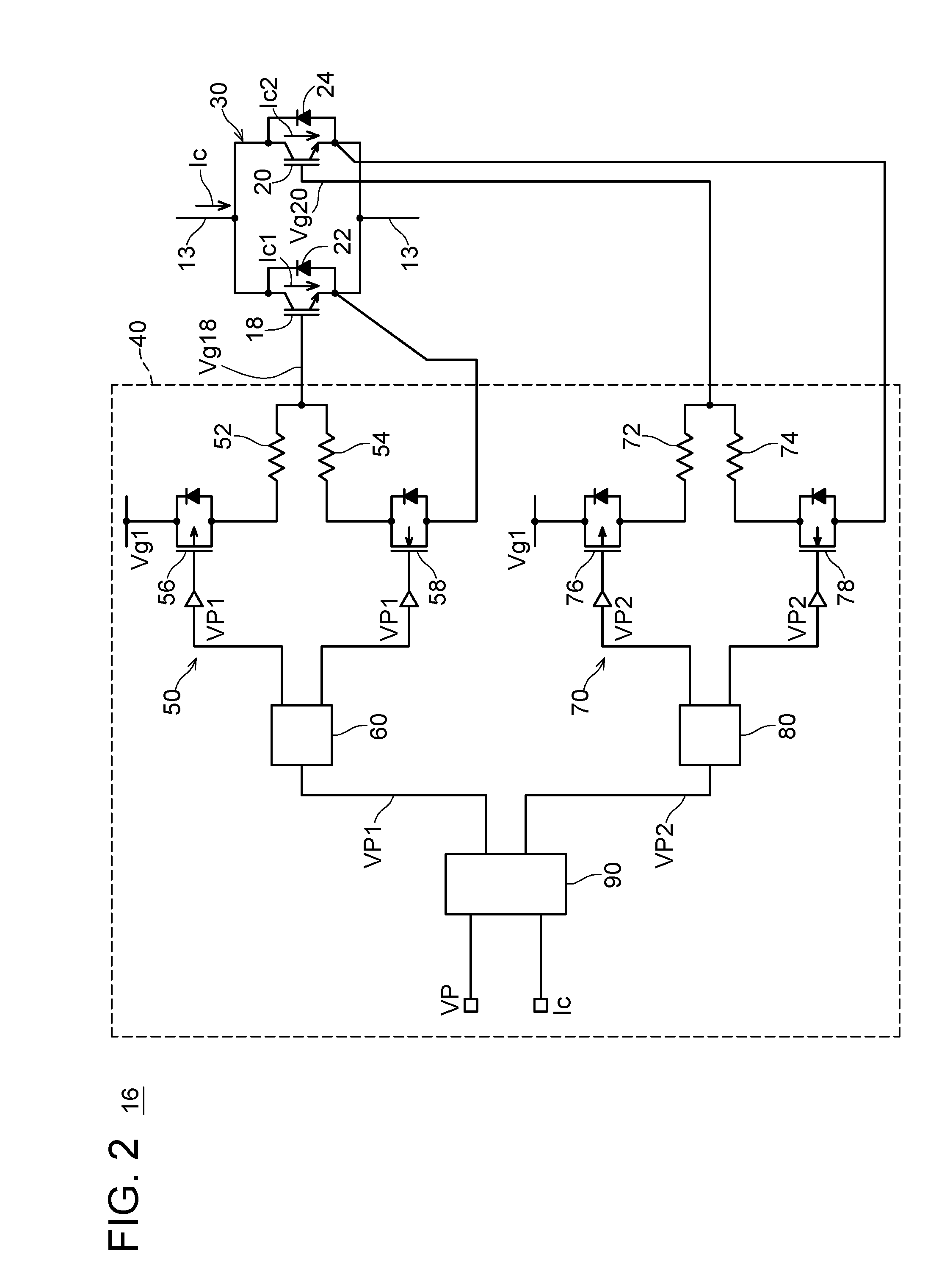
[0040]The switching circuit of the second embodiment has the same configuration as the switching circuit of the first embodiment shown in FIG. 2 except for a part of a control method. The switching circuit of the second embodiment performs control in the same manner as the switching circuit of the first embodiment when the current Ic is large. That is, when the current Ic is large, both of the IGBTs 18 and 20 are turned on in the on-period Ton and both of the IGBTs 18 and 20 are turned off in the off-period Toff. When the current Ic is small, the switching circuit of the second embodiment executes a control method different from the control method of the first embodiment.
[0041]The switching circuit of the second embodiment executes the second control procedure shown in FIG. 5 when the current Ic is small. That is, when the current Ic is small, the logic control circuit 90 controls the IGBT 18 and the IGBT 20 so that an on-period Ton 18 during which only the IGBT 18 is turned on and ...
third embodiment
[0042]The switching circuit of the third embodiment has the same configuration as that of the switching circuit of the first embodiment shown in FIG. 2 except for a part of a control method. The switching circuit of the third embodiment performs control in the same manner as the switching circuit of the first embodiment when the current Ic is large. When the current Ic is small, the switching circuit of the third embodiment executes a control method different from the control method of the first embodiment.
[0043]The switching circuit of the third embodiment executes the second control procedure shown in FIG. 6, when the current Ic is small. The logic control circuit 90 turns on both of the IGBTs 18 and 20 at the turn-on timing tn even when the current Ic is small. Then, the IGBT 20 is turned off at a timing tc just before the turn-off timing tf. After that, the logic control circuit 90 maintains the IGBT 20 in the off-state until a next turn-on timing tn (that is, until the turn-off...
PUM
 Abstract
Description
Claims
Application Information