Switching circuit

a technology of switching circuit and switch, which is applied in the direction of electronic switching, dc-ac conversion without reversal, pulse technique, etc., can solve the problems of difficult to reduce the turn-off loss of the igbt, the switching speed and the turn-off loss are not established, and the switch speed is increased. , to achieve the effect of reducing gate resistance, reducing turn-off loss, and increasing the switching speed of the igb

Active Publication Date: 2017-06-27
TOYOTA JIDOSHA KK
View PDF7 Cites 6 Cited by
  • Summary
  • Abstract
  • Description
  • Claims
  • Application Information

AI Technical Summary

Benefits of technology

[0006]In a switching circuit that utilizes an IGBT, a turn-off loss that is caused in the IGBT presents a problem. Conventionally, it is known that the switching speed of the IGBT is increased by reducing the gate resistance, and that the turn-off loss decreases when the switching speed is increased (i.e., when the gate resistance is reduced). However, the inventors have confirmed that the aforementioned relationship between the switching speed and the turn-off loss is not established in the case where the current flowing through the IGBT is small. That is, the inventors have confirmed that it is difficult to reduce the turn-off loss of the IGBT at the time of the flow of a small current by reducing the gate resistance. Accordingly, the present specification provides a new art for reducing the turn-off loss of the IGBT at the time of the flow of a small current.
[0007]The inventors have confirmed that while there is such a relationship that the turn-off loss decreases as the size of the IGBT decreases in the case where the current flowing through the IGBT is small, the relationship between the size of the IGBT and the turn-off loss disappears when the current flowing through the IGBT becomes large. The disclosure reduces the turn-off loss of the IGBT with the aid of this phenomenon.
[0015]When the current flowing through the wiring is small, the second control procedure is executed. In the second control procedure, the second target IGBT turns off prior to the turn-off timing. Accordingly, at the turn-off timing, the first target IGBT turns off with the second target IGBT already off. In this case, the size of the IGBT that turns off is the size of the first target IGBT. Therefore, the size of the IGBT that turns off is smaller than in the first control procedure. In the second control procedure, the current flowing through the wiring is small, so the turn-off loss can be reduced by turning off the first target IGBT with the second target IGBT off (i.e., reducing the size of the IGBT that turns off). Besides, in the second control procedure, the second target IGBT is off and the first target IGBT is on at least immediately before the turn-off timing. Therefore, a current flows through the first target IGBT without flowing through the second target IGBT. However, the current flowing through the wiring is small. Therefore, even when a current thus flows through the first target IGBT in a biased manner, no excessive load is applied to the first target IGBT.
[0016]As described hitherto, according to this switching circuit, the turn-off loss at the time of the flow of a small current can be reduced while reducing the loads applied to the respective IGBT's at the time of the flow of a large current.

Problems solved by technology

In a switching circuit that utilizes an IGBT, a turn-off loss that is caused in the IGBT presents a problem.
However, the inventors have confirmed that the aforementioned relationship between the switching speed and the turn-off loss is not established in the case where the current flowing through the IGBT is small.
That is, the inventors have confirmed that it is difficult to reduce the turn-off loss of the IGBT at the time of the flow of a small current by reducing the gate resistance.
Therefore, the size of the IGBT's that turn off is large.
However, in the first control procedure, the current flowing through the wiring (i.e., the first IGBT and the second IGBT) is large, so there is hardly any correlation between the size of the IGBT's that turn off and the turn-off loss.
However, the current flowing through the wiring is small.

Method used


Image

  • Switching circuit
  • Switching circuit
  • Switching circuit

Examples


first embodiment

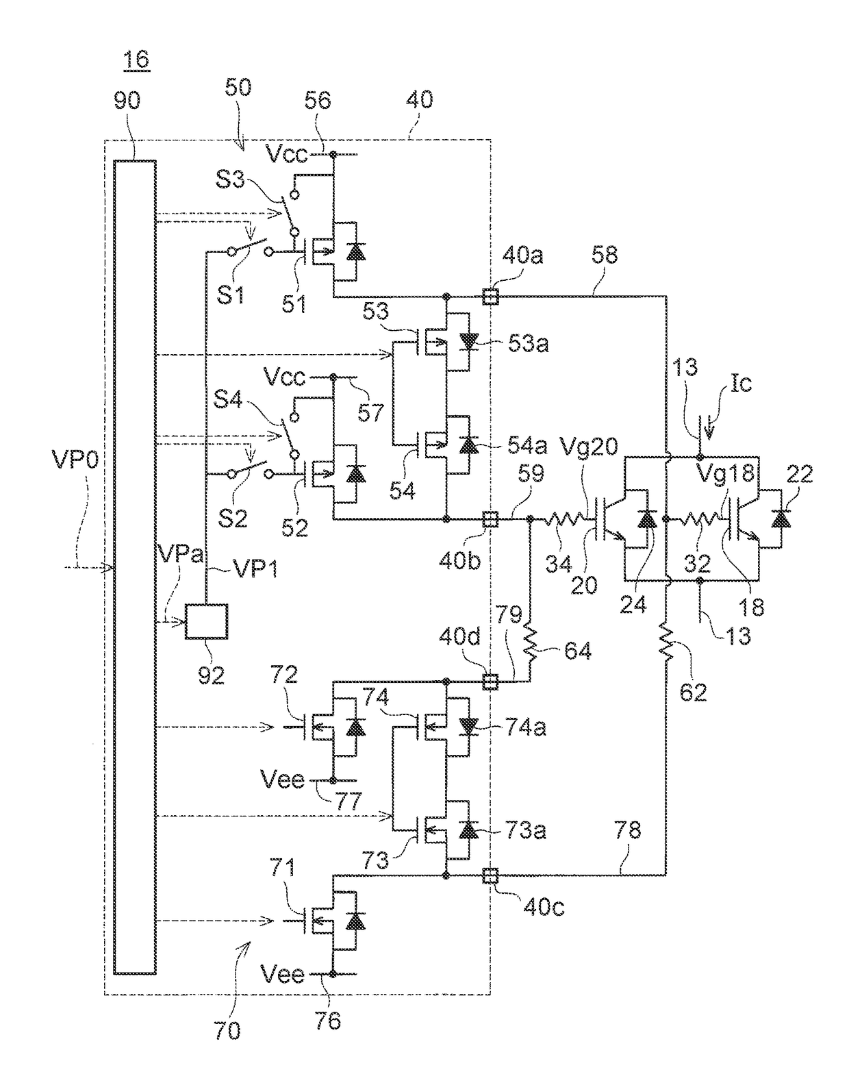
[0032]The inverter circuit 10 in the disclosure shown in FIG. 1 supplies an alternating current to a running motor 98 of a vehicle. The inverter circuit 10 has a high-potential wiring 12 and a low-potential wiring 14. The high-potential wiring 12 and the low-potential wiring 14 are connected to a direct-current electric power supply (not shown). A high potential VH is applied to the high-potential wiring 12, and a low potential VL is applied to the low-potential wiring 14. Three series circuits 15 are connected in parallel between the high-potential wiring 12 and the low-potential wiring 14. Each of the series circuits 15 has a connection wiring 13 that is connected between the high-potential wiring 12 and the low-potential wiring 14, and has two of the switching circuits 16 that are interposed in the connection wiring 13. The two switching circuits 16 are connected in series between the high-potential wiring 12 and the low-potential wiring 14. Output wirings 22a to 22c are connecte...

second embodiment

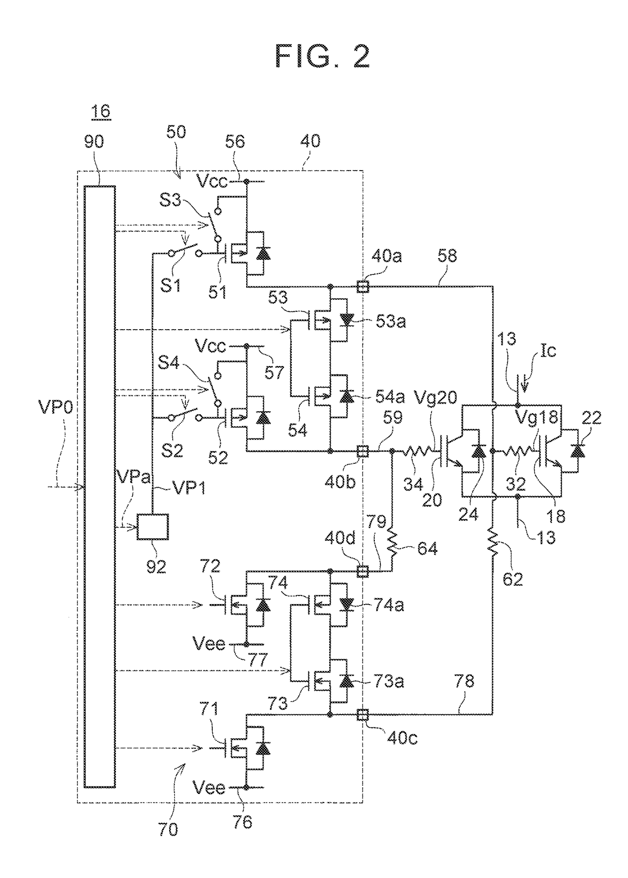
[0087]In the case where the current Ic is small, the switching circuit according to the disclosure executes the unilateral control procedure as shown in FIG. 5. That is, in the case where the current Ic is small, the logic circuit 90 controls the IGBT's 18 and 20 such that an on period Ton18 when only the IGBT 18 turns on and an on period Ton20 when only the IGBT 20 turns on alternately emerge. More specifically, the logic circuit 90 performs control such that the on period Ton18, the off period Toff, the on period Ton20 and the off period Toff repeatedly emerge in this sequence. In the off period Toff, both the IGBT 18 and the IGBT 20 are off. For example, the logic circuit 90 determines at a timing t1 in FIG. 5 that the current Ic is smaller than the threshold Ith in the immediately preceding on period Ton20. Then, in the subsequent on period Ton18, the logic circuit 90 turns on the IGBT 18 and holds the IGBT 20 off. Since the current Ic has not risen to the threshold Ith in this ...

third embodiment

[0094]In the aforementioned control, while the IGBT 20 turns off at the timing tc, the IGBT 18 is held on. Even when the IGBT 20 turns off, the IGBT 18 is on, so the voltage between the collector and emitter of the IGBT 20 is held equal to a low voltage. Accordingly, when the IGBT 20 turns off, no turn-off loss is caused. Besides, when the IGBT 18 turns off at the turn-off timing tf, the voltage between the collector and emitter of the IGBT 18 rises due to the turning off of the IGBT 18. Accordingly, the turn-off loss is caused at the turn-off timing tf. However, at the turn-off timing tf, the IGBT 18 turns off alone, so the turn-off loss is small. Accordingly, the switching circuit according to the disclosure also makes it possible to reduce the turn-off loss. Besides, even in the case where the current Ic is small as described hitherto, the loads applied to the IGBT's 18 and 20 can be further reduced by scattering the current Ic to the IGBT's 18 and 20 in part of the on period Ton...


PUM


Abstract

A switching circuit switches a first IGBT and a second IGBT. A control circuit is equipped with a first switching element that is configured to be able to control a gate current of the first IGBT, a second switching element that is configured to be able to control a gate current of the second IGBT, and a third switching element that is connected between an electrode of the first IGBT and an electrode of the second IGBT. The control circuit controls a turn on timing and turn off timing.

Description

INCORPORATION BY REFERENCE[0001]The disclosure of Japanese Patent Application No. 2015-227860 filed on Nov. 20, 2015 including the specification, drawings and abstract is incorporated herein by reference in its entirety.BACKGROUND[0002]1. Field of the Disclosure[0003]The disclosure relates to a switching circuit.[0004]2. Description of Related Art[0005]A switching circuit that utilizes a plurality of IGBT's is disclosed in Japanese Patent Application Publication No. 2004-112916 (JP 2004-112916 A). The IGBT's can switch a large current.SUMMARY[0006]In a switching circuit that utilizes an IGBT, a turn-off loss that is caused in the IGBT presents a problem. Conventionally, it is known that the switching speed of the IGBT is increased by reducing the gate resistance, and that the turn-off loss decreases when the switching speed is increased (i.e., when the gate resistance is reduced). However, the inventors have confirmed that the aforementioned relationship between the switching speed ...

Claims


Application Information

Patent Timeline
Patent Type & Authority Patents(United States)
IPC IPC(8): H03K5/08H03K17/06H03K17/567H01L27/06H01L29/739H01L29/861H01L49/02H01L23/528H01L29/73
CPCH03K17/06H01L27/0635H03K17/567H01L29/861H01L23/528H01L28/20H01L29/73H01L29/7393H02M1/088H02M1/32H02M7/003H02M7/5387H02M1/0054H03K17/127H03K2217/94042H01L27/0825Y02B70/10H02M1/08H02M7/48H02P27/06H03K17/168
Inventor NA, HYOUNGJUNTOSHIYUKI, KENABOU, SHOUJI
Owner TOYOTA JIDOSHA KK
Why Eureka
Try Eureka