Semiconductor apparatus
a technology of semiconductor devices and semiconductors, applied in the direction of electrical devices, semiconductor devices, diodes, etc., can solve the problems of high turn-off loss of semiconductor devices, and achieve the effect of reducing the turn-off loss of semiconductor devices and high turn-off loss
- Summary
- Abstract
- Description
- Claims
- Application Information
AI Technical Summary
Benefits of technology
Problems solved by technology
Method used
Image
Examples
first embodiment
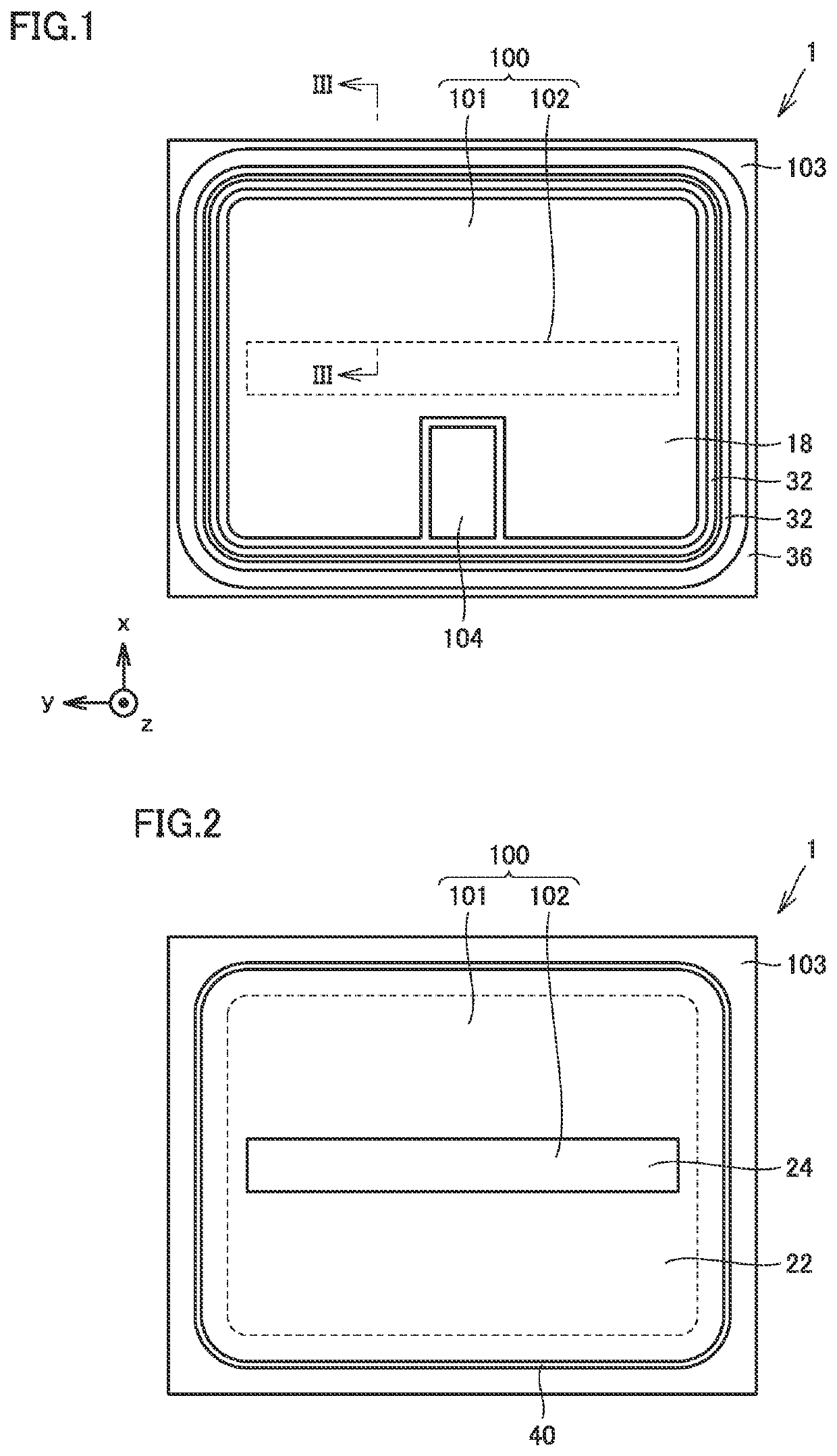
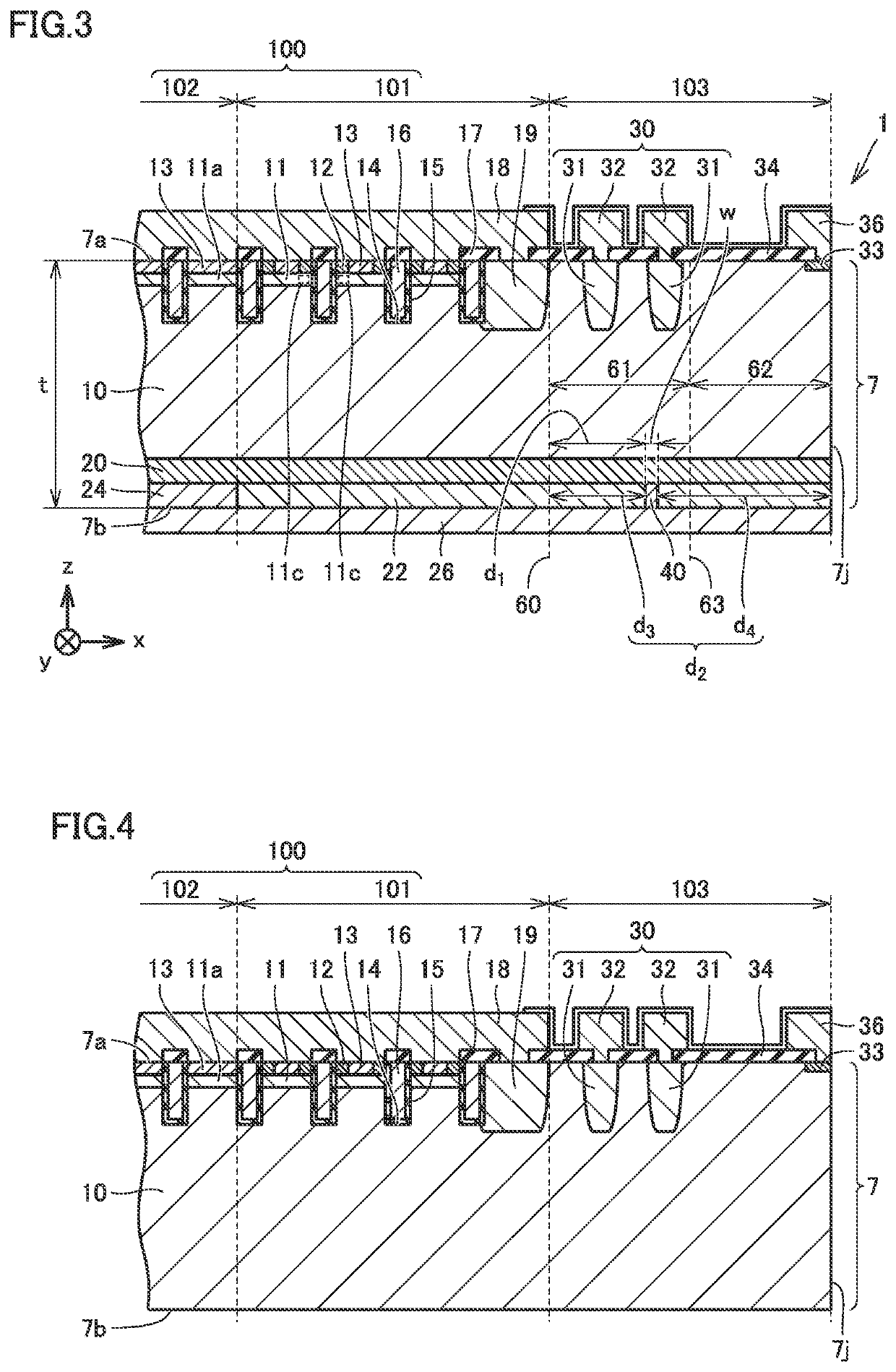
[0046]Referring to FIGS. 1 to 3, a semiconductor apparatus 1 according to a first embodiment is described. Semiconductor apparatus 1 mainly includes a semiconductor substrate 7, a first electrode 18, and a second electrode 26. Semiconductor apparatus 1 may further include a gate pad 104, a floating electrode 32, and a channel stop electrode 36.
[0047]Semiconductor substrate 7 is a silicon substrate or a silicon carbide substrate, for example. Semiconductor substrate 7 has a front surface 7a, and a back surface 7b opposite to front surface 7a. Semiconductor substrate 7 includes a device region 100, and a peripheral region 103 surrounding device region 100. Device region 100 includes a first semiconductor device region 101. A first semiconductor device is formed in first semiconductor device region 101. The first semiconductor device is an insulated gate bipolar transistor (IGBT), for example. Device region 100 may further include a p well region 19. As shown in FIG. 3, first electrode...
second embodiment
[0119]Referring to FIGS. 10 to 12, a semiconductor apparatus 1b according to a second embodiment is described. Semiconductor apparatus 1b has a similar configuration and produces a similar effect to semiconductor apparatus 1 of the first embodiment, but is different mainly on the following points.
[0120]In semiconductor apparatus 1b, n type region 40 includes a plurality of n type region portions 41 in the plan view of back surface 7b. The plurality of n type region portions 41 are arranged discretely in peripheral region 103. The plurality of n type region portions 41 are formed in a dashed line in peripheral region 103, for example. The plurality of n type region portions 41 may be formed as dots in peripheral region 103. A longitudinal length L of each n type region portion 41 may be smaller than a spacing G between two adjacent n type region portions 41. In the present embodiment, the third area ratio of n type region 40 to peripheral region 103 is lower than in the first embodim...
third embodiment
[0121]Referring to FIGS. 13 to 15, a semiconductor apparatus 1c according to a third embodiment is described. Semiconductor apparatus 1c has a similar configuration and produces a similar effect to semiconductor apparatus 1 of the first embodiment, but is different mainly on the following points.
[0122]In semiconductor apparatus 1c of the present embodiment, n type region 40 is formed as a plurality of rings surrounding device region 100 in the plan view of back surface 7b. Specifically, n type region 40 includes a plurality of n type region portions 42 and 43. Each of the plurality of n type region portions 42 and 43 surrounds device region 100. The plurality of n type region portions 42 and 43 are arranged discretely in peripheral region 103. The plurality of n type region portions 42 and 43 are spaced apart from each other. N type region portion 42 is formed at the same position as n type region 40 of the first embodiment. N type region portion 43 is formed on the inner side relat...
PUM
| Property | Measurement | Unit |
|---|---|---|
| electron concentration | aaaaa | aaaaa |
| electron concentration | aaaaa | aaaaa |
| electron concentration | aaaaa | aaaaa |
Abstract
Description
Claims
Application Information


