High K dielectric film

a dielectric film, high-k technology, applied in the direction of semiconductor devices, electrical apparatus, transistors, etc., can solve the problems of inacceptable leakage current, low current leakage of devices, and dramatic increase of leakage current with reducing the thickness of gate dielectrics

Inactive Publication Date: 2006-09-12
TAIWAN SEMICON MFG CO LTD
View PDF3 Cites 11 Cited by
  • Summary
  • Abstract
  • Description
  • Claims
  • Application Information

AI Technical Summary

Problems solved by technology

The result is that the silicon dioxide operates very effectively causing devices to have low current leakage.
Unfortunately, the leakage current increases dramatically with reduced thickness of the gate dielectric.
For example, SiO2 having a thickness of less than 20Å results in unacceptable leakage current and degraded device performance.
These grain boundaries are areas of leakage and other problems that affect electrical performance.
Thus, many of the materials being developed for high K purposes have been found to have problems because they do not have a high enough band gap or because they are difficult to make with enough integrity to prevent current leakage through the dielectric.
Additional problems remain unresolved such as thermal stability with the silicon substrate and gate electrode, fermi level pinning at the oxide / metal interface and scaling.
Even though amorphous materials including Hr-based and Zr-based oxides are being investigated, there appears to be no clear solution since there are outstanding problems with these materials when integrating into a CMOS flow.
In theory, high K dielectric films can be made typically monocrystalline, although difficulties exist.
One such difficulty is matching the crystalline structure of the film with that of the underlying semiconductor, typically silicon, as well as during the formation process that it be in fact perfectly formed.
Even with using MBE technology there is still the difficulty of ensuring defect free films.
In developing new high K dielectrics there is also another potential problem of having too high of a dielectric constant.
If the dielectric constant is too high, there is an effect that is called fringing field effect which adversely affects the performance of the transistor.
This has to do with excessive coupling between the gate and the source / drain.
In this case, the typical desirable silicon oxide equivalent thickness is between 5 and 15 angstroms but with silicon oxide of 5 to 15 angstroms it has problems with leakage, reliability, growth rate, and uniformity.
Thus, when a film is that small there can be difficulties in manufacturing it as well as using it.
High K dielectric films which include aluminum have been developed, yet aluminum is known to cause high interface state density and degraded mobility in silicon based devices.

Method used


Image

  • High K dielectric film
  • High K dielectric film
  • High K dielectric film

Examples


Embodiment Construction

[0021]The following detailed description is of exemplary embodiments only and is not intended to limit the invention or the application and uses of the invention. Rather, the following description provides a convenient illustration for implementing exemplary embodiments of the invention. Various changes to the described embodiments may be made in the function and arrangement of the elements described without departing from the scope of the invention as set forth in the appended claims. A high K dielectric film comprising lanthanum, lutetium, and oxygen provides an excellent candidate material for replacement of silicon dioxide. It combines the advantages of having a desirable range of dielectric constant, the ability to remain amorphous at high temperatures, and provides for low leakage.

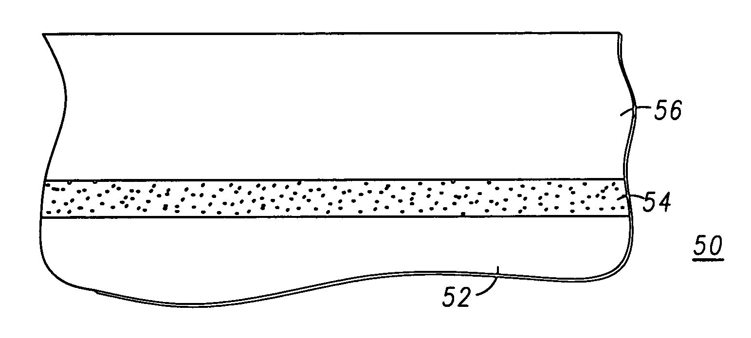
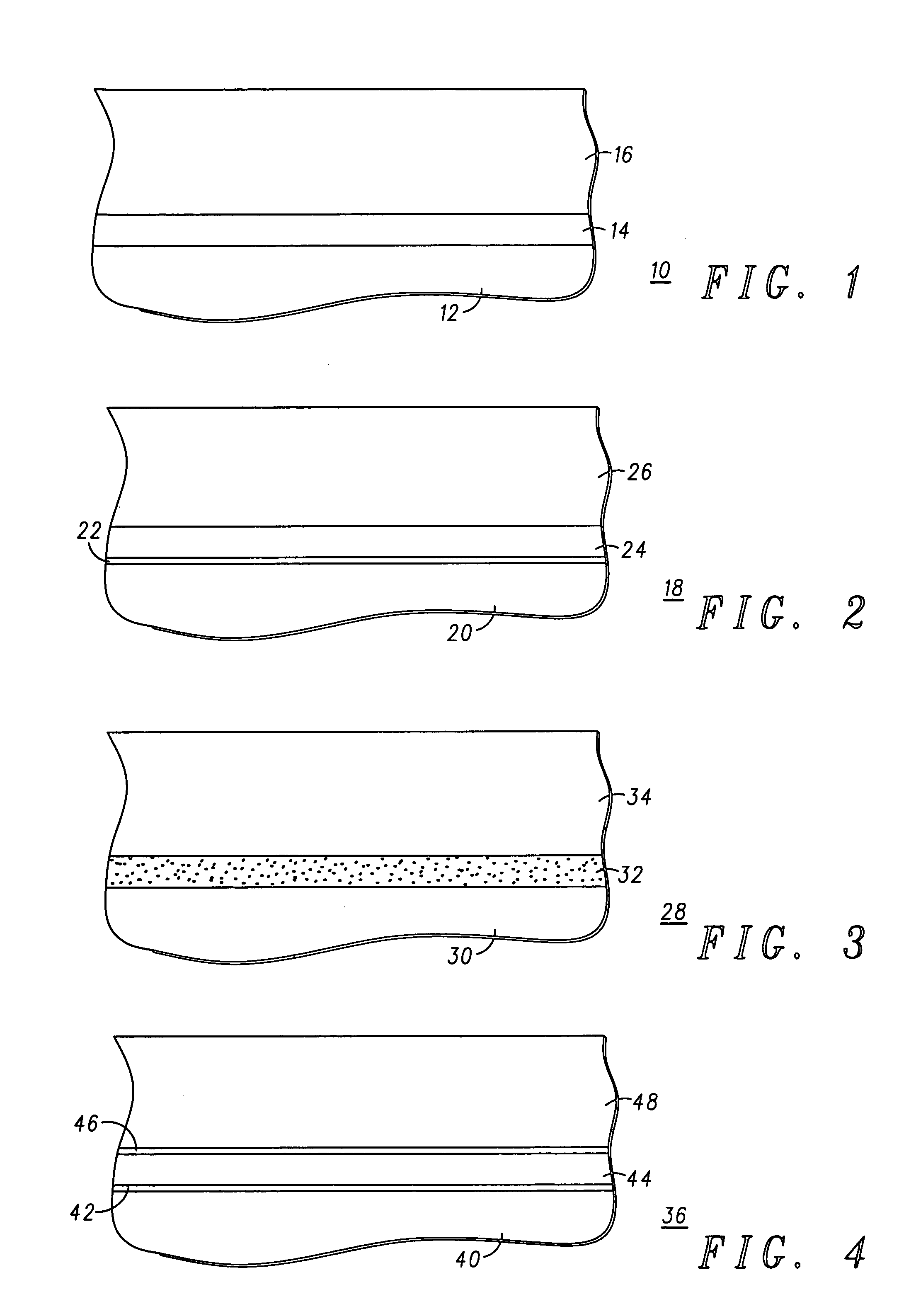
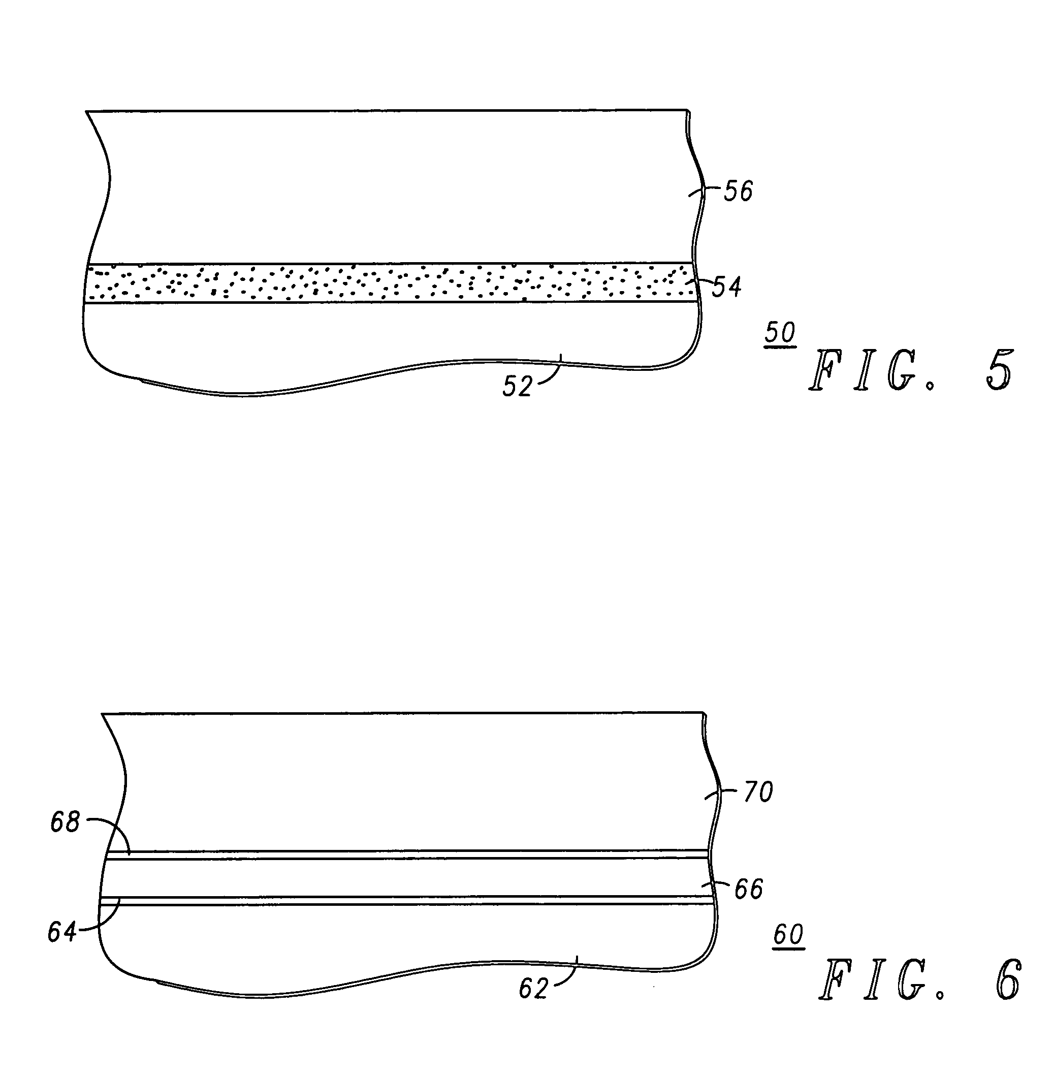
[0022]Shown in FIG. 1 is a portion 10 of an integrated circuit having a substrate 12 of semiconductor material, a dielectric film 14 and a conductive film 16. Substrate 12 has a semiconductor region ...


PUM


Abstract

A dielectric layer comprised of lanthanum, lutetium, and oxygen that is formed between two conductors or a conductor and a substrate. In one embodiment, the dielectric layer is formed over the substrate without the need for an additional interfacial layer. In another embodiment, the dielectric layer is graded with respect to the lanthanum or lutetium content or in the alternative, may include aluminum. In yet another embodiment, an insulating layer is formed between the conductor or substrate and the dielectric layer or between both the conductor and substrate and the dielectric layer. The dielectric layer is preferably formed by molecular beam epitaxy, but can also be formed by atomic layer chemical vapor deposition, physical vapor deposition, organometallic chemical vapor deposition or pulsed laser deposition.

Description

FIELD OF THE INVENTION[0001]This invention relates to devices used in and methods for making integrated circuits, and more particularly to high K dielectrics used in making integrated circuits. This application claims benefit of U.S. Ser. No. 60 / 519,765 filed Nov. 12, 2003.BACKGROUND OF THE INVENTION[0002]CMOS devices contain both n- and p- channel field effect transistors (FET) and form the basis of integrated circuits. These transistors are metal oxide-based semiconductor devices which include a source and drain region and an insulated gate in between. As the density of integrated circuits and performance increases, the dimensions of the transistors have to be reduced. As a result the thickness of the insulated gate dielectric layer has to be made smaller. With regard to gate dielectrics, one of the desirable features of the dielectric layer is that it couple the overlying gate electrode to the underlying channel so that the channel is responsive to the stimulus applied to the gat...

Claims


Application Information

Patent Timeline
Patent Type & Authority Patents(United States)
IPC IPC(8): H01L29/76H01L21/28H01L29/49H01L29/51
CPCH01L21/02192H01L21/02194H01L21/02269H01L21/28194H01L21/31604H01L29/513H01L29/518H01L29/4908H01L29/517H01L21/28273H01L29/40114H01L21/31
Inventor DROOPAD, RAVINDRANATH
Owner TAIWAN SEMICON MFG CO LTD
Why Eureka
Try Eureka