Differential signal squelch detection circuit and method

a detection circuit and signal technology, applied in the direction of digital transmission, line-fault/interference reduction, baseband system details, etc., can solve the problem that the output of the loss is often too slow to reliably detect the squelch sta

Inactive Publication Date: 2006-10-10
AGILENT TECH INC
View PDF16 Cites 10 Cited by
  • Summary
  • Abstract
  • Description
  • Claims
  • Application Information

AI Technical Summary

Problems solved by technology

As a result, electronic devices connected to such a bus are usually required to detect the squelch state of the differential pair, which generally only lasts for a few tens or hundreds of nanoseconds.
However, the primary purpose of the LOS output is to detect catastrophic failures of the communication links, such as the signal wires of the differential pair being physically disconnected.
As a result, the LOS output often reacts too slowly to reliably detect the squelch state.
Unfortunately, since the circuit of FIG. 1 is actually detecting the presence or absence of signal transition activity, as opposed to the presence of the squelch state, extended periods of time during which the differential pair resides at their proper +V or −V levels without transition will be incorrectly interpreted as squelch.
Unfortunately, most high-speed comparators, which would be required in the case of a high-speed serial bus, are designed with minimal hysteresis to facilitate higher signal switching frequencies.

Method used


Image

  • Differential signal squelch detection circuit and method
  • Differential signal squelch detection circuit and method
  • Differential signal squelch detection circuit and method

Examples


Embodiment Construction

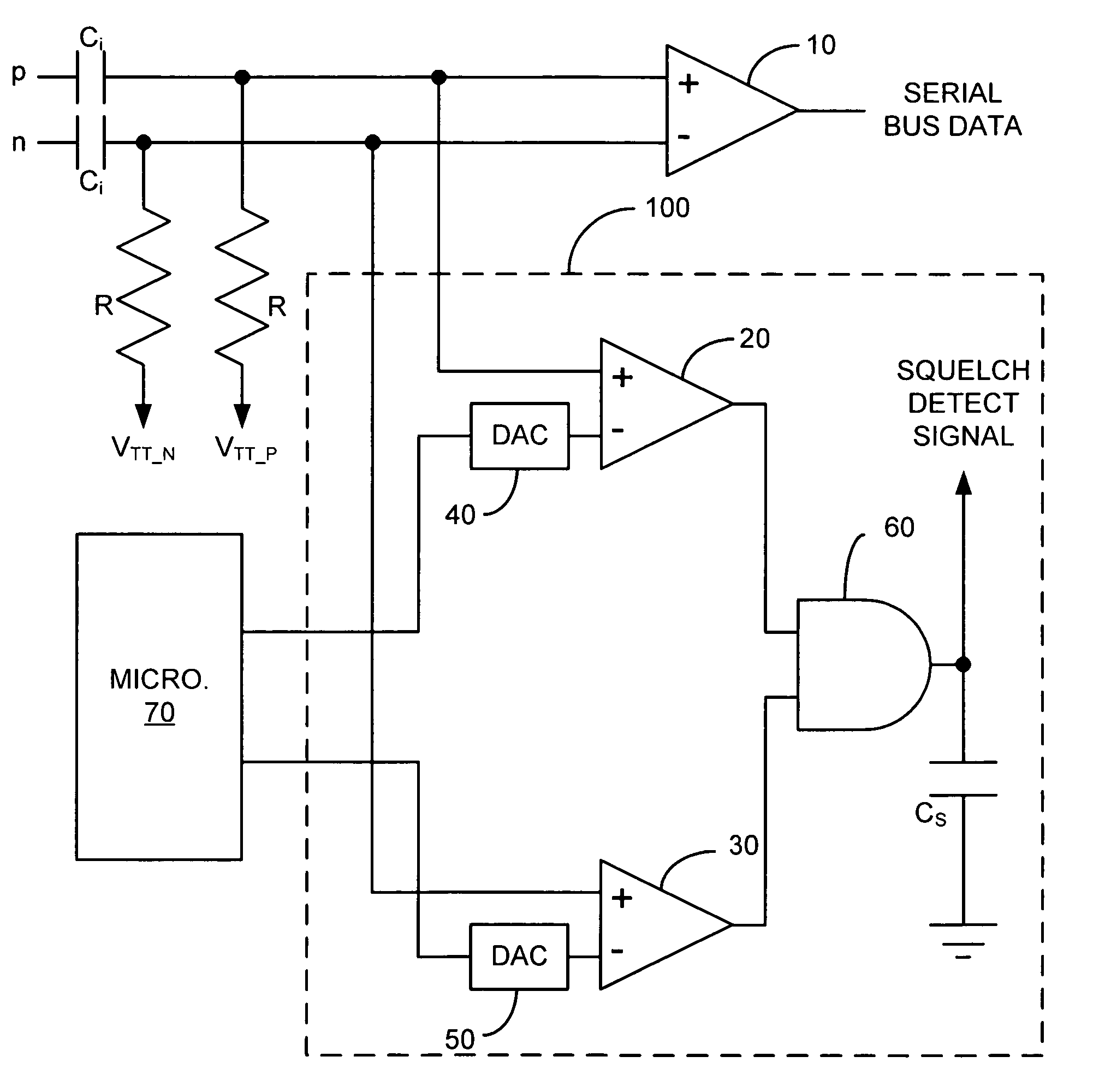
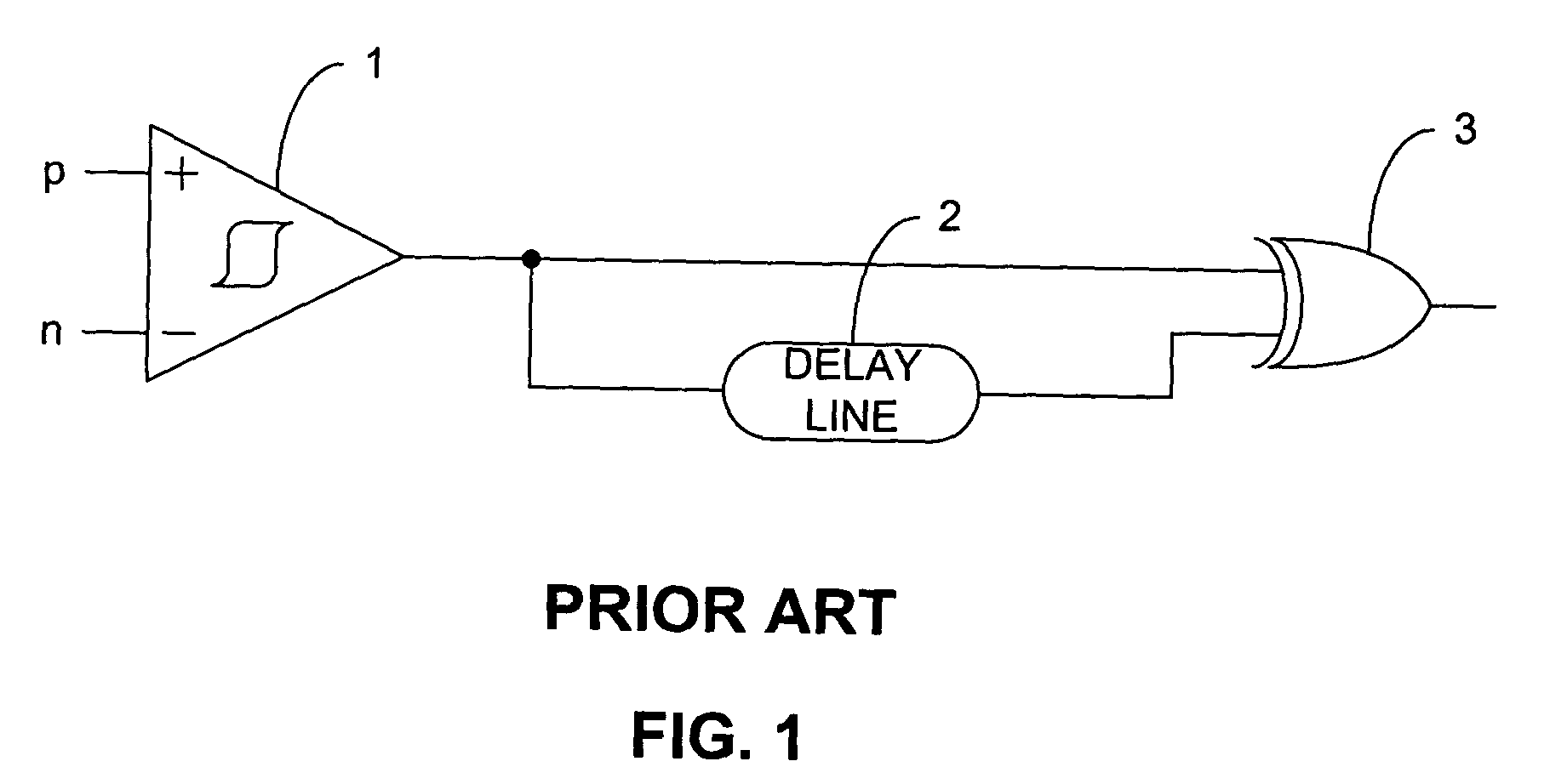
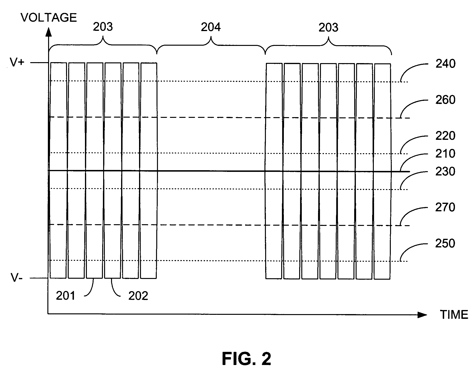
[0016]Before describing specific embodiments of the invention, a short discussion of the actions of the differential signal lines, “p” and “n”, during both the data transfer state and squelch, or out-of-band, state is desirable. As stated earlier, squelch state essentially is the state in which the “p” and “n” signal lines are not being driven to their normal data transmission voltage levels.

[0017]FIG. 2 graphically displays in an idealized fashion the action of the differential signal lines when in the data transfer state 203 and while in the squelch state 204. In typical differential signal fashion, the “p” signal waveform 201 and the “n” signal waveform 202, during the data transfer state 203, are essentially mirror images of each other across a midpoint voltage 210, existing substantially halfway between voltage levels V+ and V−. In other words, while the voltage of “p” signal waveform 201 is at V+, the voltage of the “n” signal waveform 202 is at V−, and vice-versa. To ensure t...


PUM


Abstract

An electrical circuit detects a “squelch,” or “out-of-band,” state of a differential signal pair having a positive (“p”) signal line and a negative (“n”) signal line. In one embodiment of the invention, a first and a second comparator each have positive inputs driven by the positive and negative signal lines, respectively. The negative inputs of the comparators are driven by the outputs of separate digital-to-analog converters (DACs) which are set to a lower squelch threshold voltage. The outputs of the comparators then drive the inputs of a logical AND gate, the output of which indicates the current squelch state of the differential signal pair.

Description

BACKGROUND OF THE INVENTION[0001]Several modern high-speed serial data busses, normally used for digital communication between physically separated electronic devices, implement the well-known, time-tested “differential pair” signal line configuration to transmit and receive data. The differential pair typically consists of two signal lines, a positive (“p”) signal line and a negative (“n”) signal line, which normally exhibit opposite voltage polarities during normal data transmission. For example, a data value of ‘1’ is usually indicated on a differential pair with a voltage V+ on the “p” line, and a lower voltage V− on the “n” line. Similarly, to indicate a data value of ‘0’, the “p” line would hold a voltage of V− while the “n” line would exhibit a voltage of V+. Therefore, except during times in which the data value of the differential pair is in transition, the magnitude of the differential voltage between the two signal wires generally remains at about V+ minus V−. Use of a di...

Claims


Application Information

Patent Timeline
Patent Type & Authority Patents(United States)
IPC IPC(8): H04B1/10H04B1/00H04L25/02H04L25/08
CPCH04L25/085H04L25/0276H04L25/0292
Inventor WOOD, GLENN
Owner AGILENT TECH INC
Why Eureka
Try Eureka