Method and apparatus for the monitoring and control of a semiconductor manufacturing process
What is AI technical title?
AI technical title is built by Patsnap AI team. It summarizes the technical point description of the patent document.
a semiconductor manufacturing and monitoring technology, applied in the field of semiconductor processing systems, can solve the problems of complex monitoring and control, difficult to detect early stage abnormalities and characteristic deterioration of a process, and inability to simply refer to the process data displayed
Inactive Publication Date: 2006-10-17
TOKYO ELECTRON LTD
View PDF14 Cites 99 Cited by
Summary
Abstract
Description
Claims
Application Information
AI Technical Summary
This helps you quickly interpret patents by identifying the three key elements:
Problems solved by technology
Method used
Benefits of technology
Benefits of technology
[0007]Accordingly, it is an object of the present invention to provide an Advanced Process Control (APC) system for controlling a processing tool in a semiconductor processing environment, where the APC system comprises an APC server providing a plurality of APC related applications; an Interface Server (IS) coupled to the APC server; a database coupled to the IS and APC server; and a GUI component coupled to the APC server, wherein the IS comprises means for coupling to a processing tool, and means for coupling to a plurality of process modules coupled to the processing tool.
[0008]In addition, it is an object of the present invention to provide a method for using an Advanced Process Control (APC) system for controlling a processing tool in a semiconductor processing environment, the method comprising: providing an APC server providing a plurality of APC related applications; providing an Interface Server (IS) coupled to the APC server; providing a database coupled to the IS and APC server; and providing a GUI component coupled to the APC server, wherein the IS comprises means for coupling to a processing tool, and means for coupling to a plurality of process modules coupled to the processing tool.
Problems solved by technology
Processing conditions change over time with the slightest changes in critical process parameters creating undesirable results.
In many cases, changes of process data reflecting deterioration of processing characteristics cannot be detected by simply referring to the process data displayed.
It is difficult to detect early stage abnormalities and characteristic deterioration of a process.
Inefficient monitoring of a facility can result in facility downtimes that add to the overall operational cost.
Method used
Image
Click on the blue label to locate the original text in one second.
Reading with bidirectional positioning of images and text.
Examples
Embodiment Construction
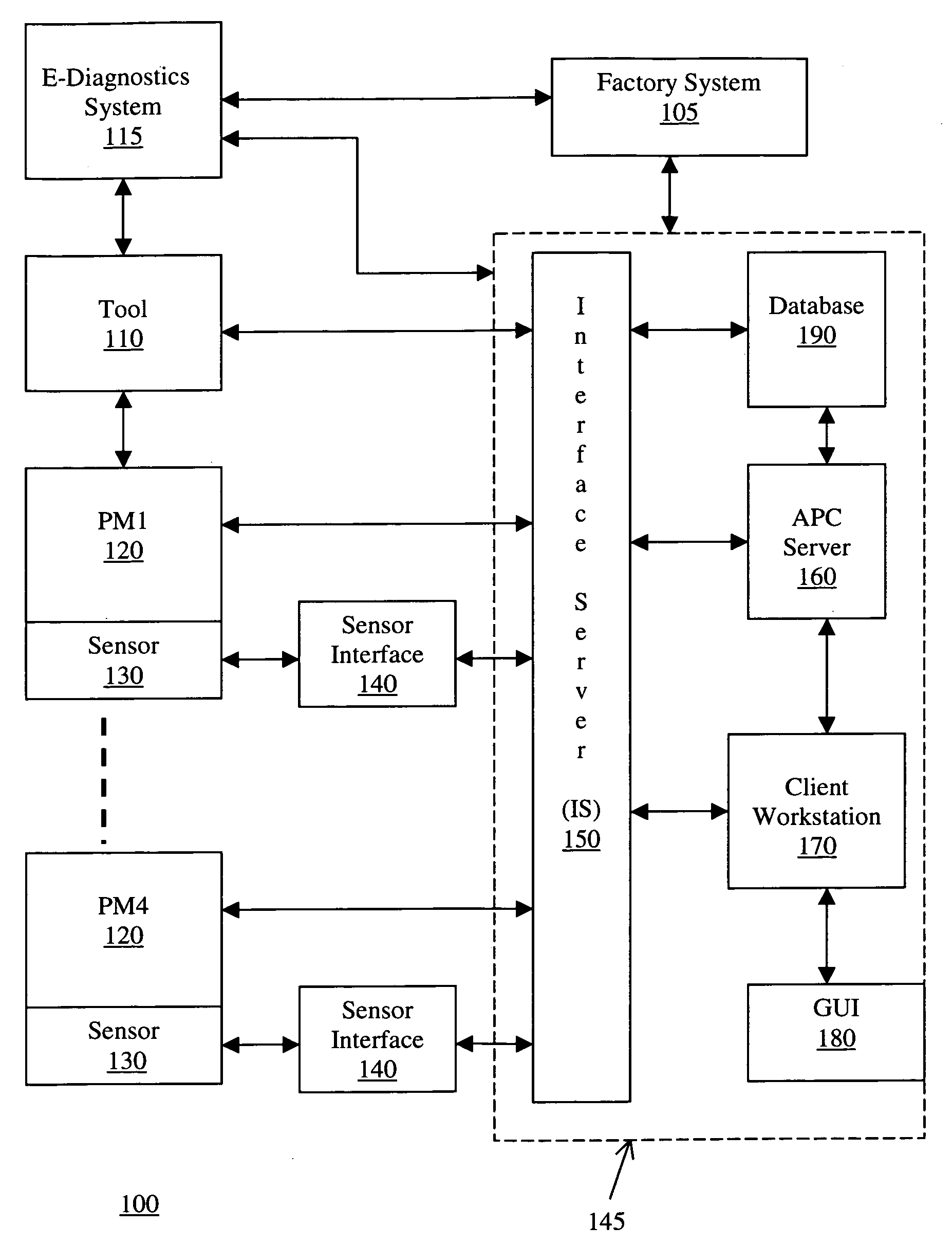
[0022]FIG. 1 shows an exemplary block diagram of an APC system in a semiconductor manufacturing environment in accordance with one embodiment of the present invention. In the illustrated embodiment, semiconductor manufacturing environment 100 comprises at least one semiconductor processing tool 110, multiple process modules 120, PM1 through PM4, multiple sensors 130 for monitoring the tool, the modules, and processes, sensor interface 140, and APC system 145. APC system 145 can comprise interface server (IS) 150, APC server 160, client workstation 170, GUI component 180, and database 190. In one embodiment, IS 150 can comprise a real-time memory database that can be viewed as a “Hub”.
[0023]APC system 145 can comprise a tool level (TL) controller (not shown) for controlling at least one of a processing tool, a process module, and a sensor.
[0024]In the illustrated embodiment, a single tool 110 is shown along with four process modules 120, but this is not required for the invention. Th...
PUM
Abstract
An Advanced Process Control (APC) system including Graphical User Interfaces (GUIs) is presented for monitoring and controlling a semiconductor manufacturing process that is performed by a semiconductor processing system. The semiconductor processing system includes a number of processing tools, a number of processing modules (chambers), and a number of sensors, and the APC system comprises an APC server, database, interface server, client workstation, and GUI component. The GUI is web-based and is viewable by a user using a web browser.
Description
CROSS-REFERENCE TO RELATED APPLICATIONS[0001]This is a Continuation Application of International Application No. PCT / US03 / 29980, filed Sep. 25, 2003, which relies for priority upon U.S. Provisional Application No. 60 / 414,425, filed Sep. 30, 2002, the contents of both of which are incorporated herein by reference in their entireties.[0002]The present application is related to co-pending applications U.S. Continuation of PCT Application No. 10 / 951,161, filed on Sep. 28, 2004, which relies for priority upon U.S. Provisional Application No. 60 / 368,162, filed on Mar. 29, 2002; U.S. Continuation of PCT Application No. 10 / 966,112, filed Oct. 18, 2004, which relies for priority upon U.S. Provisional Application No. 60 / 374,486, filed on Apr. 23, 2002; U.S. Continuation of PCT Application No. 10 / 987,194, filed Nov. 15, 2004, which relies for priority upon U.S. Provisional Application No. 60 / 383,619, filed on May 29, 2002; U.S. Continuation of PCT Application No. 11 / 025,227, filed Dec. 30, 200...
Claims
Application Information
Patent Timeline
Application Date:The date an application was filed.
Publication Date:The date a patent or application was officially published.
First Publication Date:The earliest publication date of a patent with the same application number.
Issue Date:Publication date of the patent grant document.
PCT Entry Date:The Entry date of PCT National Phase.
Estimated Expiry Date:The statutory expiry date of a patent right according to the Patent Law, and it is the longest term of protection that the patent right can achieve without the termination of the patent right due to other reasons(Term extension factor has been taken into account ).
Invalid Date:Actual expiry date is based on effective date or publication date of legal transaction data of invalid patent.

