Apparatus and process for determination of dynamic scan field curvature

a dynamic scan field and apparatus technology, applied in the field of semiconductor manufacturing, can solve the problems of reduced product yield, over-all focus budget, and difficult control of lithography processes

Inactive Publication Date: 2006-10-24
LITEL INSTR
View PDF17 Cites 19 Cited by
  • Summary
  • Abstract
  • Description
  • Claims
  • Application Information

AI Technical Summary

Benefits of technology

[0017]A series of lithographic exposures is performed on a resist coated silicon wafer using a photolithographic scanner. The lithographic exposures produce an array of focusing fiducials that are displaced relative to each other in a unique way. The focusing fiducials are measured and the FPD computed. The resulting measurements are fed into a computer algorithm that calculates the dynamic scanning field curvature in an absolute sense in the presence of wafer height variation and other wafer / reticle stage irregularities. Alternative embodiments of the preferred embodiment allow for the determination of dynamic scanning field curvature for scanning systems with asymmetric exposure fields.

Problems solved by technology

High NA lithography has led to improved resolution and a reduction in the overall focus budget, making lithography processes difficult to control.
Poor lithographic process control (focus and exposure) leads to smaller product yields, increased manufacturing costs, and poor time to market.
While semiconductor lithographers have discovered creative reticle enhancement techniques (RETs) and other optical techniques (PSM) to increase the useable DoF—the problem remains.
While focusing error causes reduction in image fidelity, the coupling of focus error and other lens aberrations (distortions) degrades overlay or positional alignment as well.
The push to smaller feature sizes is gated by many physical limitations.
Continued advances in lithography equipment (higher NA systems, smaller wavelength exposure sources), RET's, resist processing, and automated process (focus and exposure) control techniques will get more difficult and remain critical.
Finally, while FPD deviation can be determined using a variety of methods, none of these methods have the ability to divide the focal error into correctable (possibly systematic) and non-correctable (possibly random) portions—especially for scanners and to further decouple the effects of wafer flatness.
While both techniques are widely accepted both techniques require complex calibrations to be performed at each field point.
One major drawback with the PSFM method is that a fairly elaborate calibration procedure (focus offset vs. overlay shift for each field point) is required before it can be used, the PSFM technique is rather sensitive to the source-sigma (Na-source / Na-objective) that varies from process to process.
While the PSFM method provides an FPD map across a scanner or stepper field it does not provide a method for determining the dynamic lens field curvature independent of wafer height variation in the presence of stage synchronization error.
Defocus of the tool results in an apparent shift of the center of the alignment mark relative to that of the ‘best focus’ position.
In addition, the method uses fast and accurate optical overlay tools to measure the Schnitzl patterns (in several forms, CD targets or Overlay targets, FIGS. 8–9) after wafer processing, this saves monitoring costs because optical overlay tools are less expensive to operate as compared with a CD-SEM.
Performing extra exposures during production runs is very costly.
Further, and common to all these methods, the contributions of wafer height, lens aberrations (in the form of lens field curvature), and stage synchronization are not resolved into their distinct components.

Method used


Image

  • Apparatus and process for determination of dynamic scan field curvature
  • Apparatus and process for determination of dynamic scan field curvature
  • Apparatus and process for determination of dynamic scan field curvature

Examples


first main embodiment

Discussion of First Main Embodiment

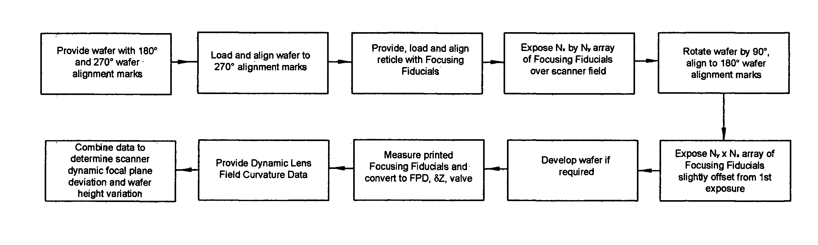
[0053]In accordance with the invention, Focusing Fiducials (FF) are exposed onto a wafer in such a manner that the effects of wafer height variations can be isolated and eliminated, and a true measure of dynamic scan FPD (SFPD) can be obtained.

[0054]A process flow diagram for the first Main Embodiment is shown in FIG. 11. A schematic of a reticle containing a (2 mx+1*2my+1) array of focusing fiducials is shown in FIG. 12. Details for the first Main Embodiment will be explained for a square exposure field (mx=my) although it is appreciated that the case of rectangular fields is a direct generalization from that description.

[0055]1. Provide Wafer

[0056]A resist coated wafer with wafer alignment marks disposed at 180° and 270° is provided (FIG. 13). The purpose of marks is to allow wafer to be inserted and aligned at two distinct notch angles that differ by +90° or −90° from one another. Depending on the scanner and FPD technology applied, the wafer no...

second main embodiment

Discussion of Second Main Embodiment

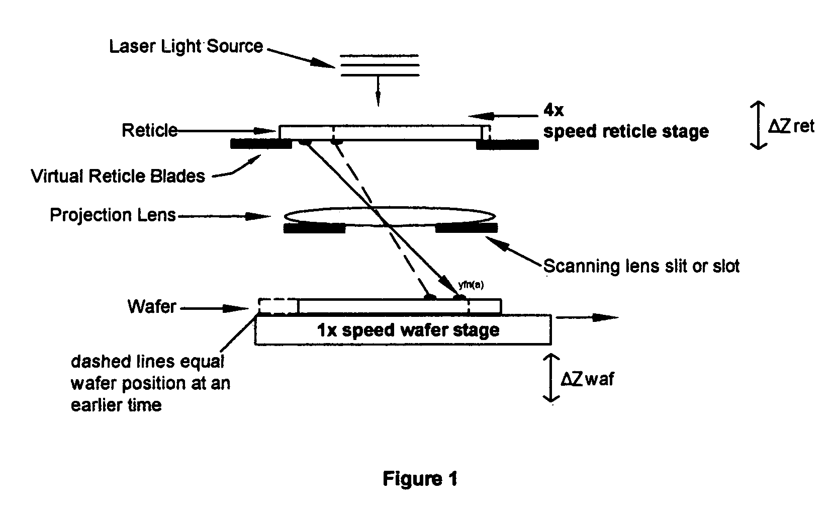
[0101]In the first Main Embodiment we have discussed in detail the practice of this invention to cases where the size of the scanned field (FX, FY) (FIG. 4) is smaller than or equal to the lesser of the slot width SW and maximum scan length SL. The present embodiment is practiced when FY (the interrogated field size in the Y direction) is greater than the maximum slot width, SW of FIG. 4. In terms of the focusing fiducials on the focusing fiducial reticle of FIG. 12, if we call the maximum number of FF's across the projected field in the X or cross scan direction NXmax and the required number of FF's in the Y or scan direction NY, when

NXmax<NY<2NXmax−1  (Equation 36)

we can apply the present embodiment. Equation 36 typically holds for scanner fields. FIG. 18 outlines the steps for carrying out the present embodiment.

[0102]Provide Wafer, Load and Align Wafer

[0103]The first two operations for the second Main Embodiment (listed as “provide wafer...


PUM

PropertyMeasurementUnit
wavelengthsaaaaaaaaaa
notch anglesaaaaaaaaaa

Abstract

A process for the determination of focal plane deviation uniquely due to the scanning dynamics associated with a photolithographic scanner is described. A series of lithographic exposures is performed on a resist coated silicon wafer using a photolithographic scanner. The lithographic exposures produce an array of focusing fiducials that are displaced relative to each other in a unique way. The resulting measurements are fed into a computer algorithm that calculates the dynamic scanning field curvature in an absolute sense in the presence of wafer height variation and other wafer / reticle stage irregularities. The dynamic scan field curvature can be used to improve lithographic modeling, overlay modeling, and advanced process control techniques related to scanner stage dynamics.

Description

BACKGROUND OF THE INVENTION[0001]1. Field of the Invention[0002]The present invention relates generally to processes for semiconductor manufacturing and, more particularly, to optical lithography techniques for the determination of focal plane deviation (FPD) associated with photolithographic projection systems.[0003]2. Description of the Related Art[0004]Semiconductor manufacturers and lithography tool vendors have been forced to produce higher numerical aperture (NA) lithography systems (steppers or scanners) using smaller wavelengths (for example, 193 nm DUV lithography) in response to the semiconductor industry's requirement to produce ever-smaller critical features. See, for example, the statement of the well-known “Moore's Law” at “Cramming more components onto integrated circuits”, G. Moore, Electronics, Vol. 38, No. 8, 1965. The ability to produce (manufacture) sub-wavelength features can often be determined by considering the rather simple (3-beam) Rayleigh scaling Resoluti...

Claims


Application Information

Patent Timeline
Patent Type & Authority Patents(United States)
IPC IPC(8): G03B27/52G03B27/42G03F7/20
CPCG03F7/70358G03F7/70516G03F7/706G03F7/70641G03F7/70791
Inventor SMITH, ADLAI H.HUNTER, JR., ROBERT O.
Owner LITEL INSTR
Why Eureka
Try Eureka